Motorola MVME172 User Manual
Page 300
5-10
Computer Group Literature Center Web Site
MCECC
5
The possible states of the bits after local, software, and power-up reset are
as defined below.
P
The bit is affected by power-up reset.
L
The bit is affected by local reset.
S
The bit is affected by software reset.
(Writing $0F to the Chip ID Register)
X
The bit is not affected by reset.
V
The effect of reset on this bit is variable.
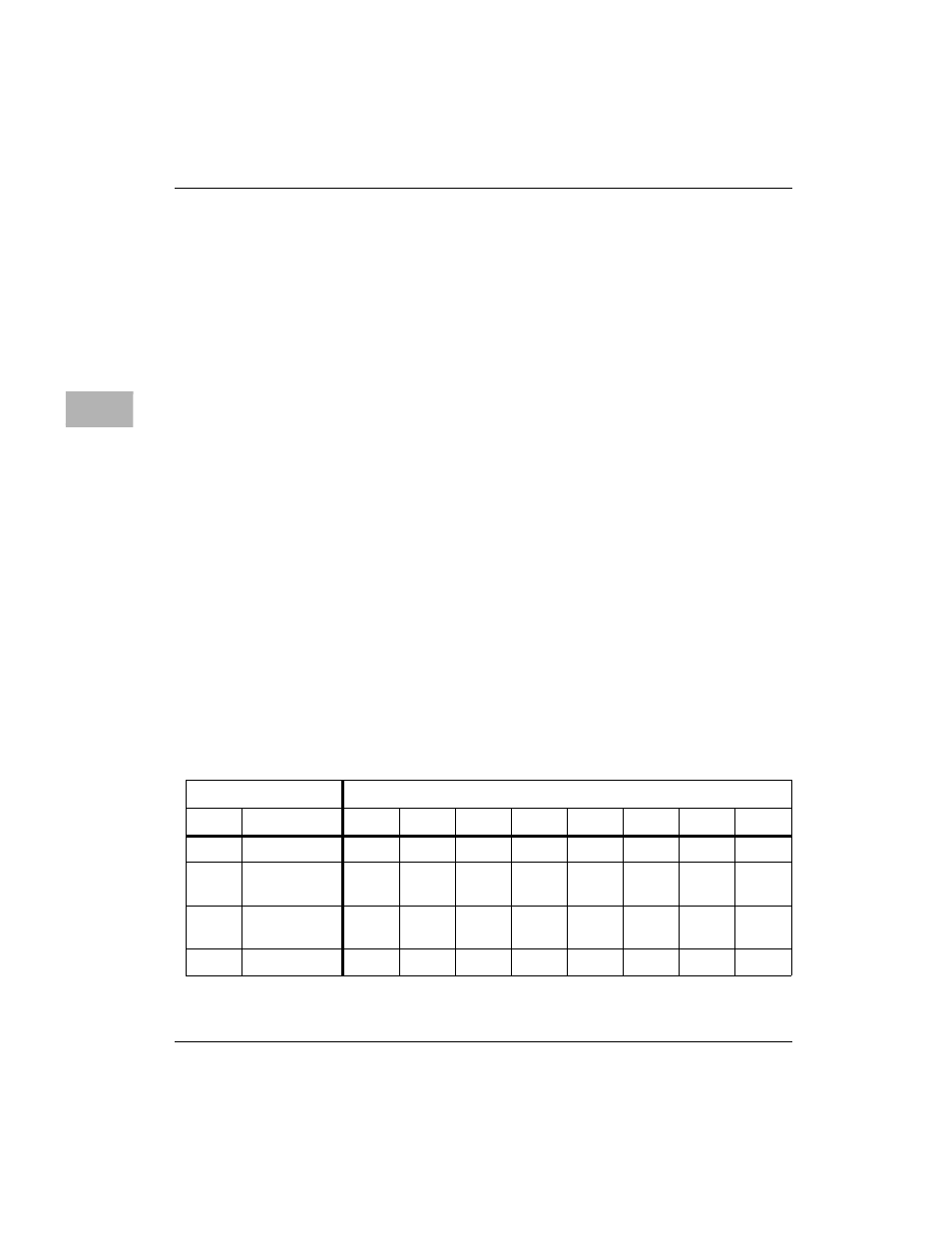
A summary of the first eight CSR registers (the ones that correspond to
those found in the MEMC040) is shown in
, following. Note that
even though there are two sets of these registers, one for the lower MCECC
and one for the upper MCECC, software should only perform read and
write cycles to the control and status registers in the upper MCECC.
Hardware takes care of duplicating the information to the lower MCECC.
The following descriptions show the upper MCECC bit positions. Upper
MCECC bit positions 31-24 correspond to lower MCECC bit positions 15-
8. The base address of the CSRs is hard coded to the address $FFF43000
for the MCECC pair on the first mezzanine board and $FFF43100 for the
MCECC pair on the second mezzanine board.
Table 5-2. MCECC Internal Register Memory Map, Part 1
MCECC Base Address = $FFF43000 (1st); $FFF43100 (2nd)
Register
Register Bit Names
Offset
Name
D31
D30
D29
D28
D27
D26
D25
D24
$00
CHIP ID
CID7
CID6
CID5
CID4
CID3
CID2
CID1
CID0
$04
CHIP
REVISION
REV7
REV6
REV5
REV47
REV3
REV2
REV1
REV0
$08
MEMORY
CONFIG
0
0
FSTRD
1
0
MSIZ2
MSIZ1
MSIZ0
$0C
DUMMY 0
0
0
0
0
0
0
0
0