Programming model, Programming model -10 – Motorola MVME172 User Manual
Page 198
3-10
Computer Group Literature Center Web Site
MC2 Chip
3
Programming Model
This section defines the programming model for the control and status
registers (CSR) in the MC2 chip. The base address of the CSR is
$FFF42000. The possible operations for each bit in the CSR are as follows:
R
This bit is a read-only status bit.
R/W
This bit is readable and writable.
C
Writing a one to this bit clears this bit or another bit. This
bit reads zero.
The possible states of the bits after local and power-up reset are as defined
below.
P
The bit is affected by power-up reset.
L
The bit is affected by local reset.
X
The bit is not affected by reset.
0
The bit is always 0.
1
The bit is always 1.
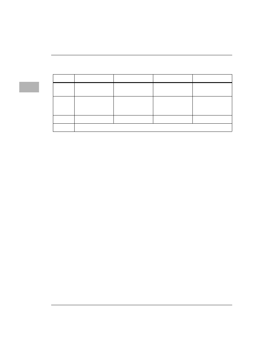
$40
Bus Clock
PROM Access
Time Control
Flash Access Time
Control
ABORT Switch
Interrupt Control
$44
RESET Switch
Control
Watchdog Timer
Control
Access &
Watchdog Time
Base Select
Reserved
$48
DRAM Control
Reserved
MPU Status
Reserved
$4C
32-bit Prescaler Count Register
Table 3-2. MC2 Chip Register Map (Continued)
Offset
D31-D24
D23-D16
D15-D8
D7-D0