Dram and sram memory controller registers, Dram space base address register, Dram and sram memory controller registers -25 – Motorola MVME172 User Manual
Page 213: Dram space base address register -25

Programming Model
http://www.mcg.mot.com/literature
3-25
3
DRAM and SRAM Memory Controller Registers
The DRAM decode logic consists of a base register, a size register, and an
options register. The SRAM decode logic consists of a similar set of
registers.
The reset logic initializes the DRAM and SRAM Base registers so that
DRAM space starts at address 0 and SRAM space starts at $FFE00000.
DRAM and SRAM are inhibited by reset. Software can examine the
MVME172 DRAM/SRAM Options Register at address $FFF42024 bits
20-16 to determine the size of the SRAM and DRAM.
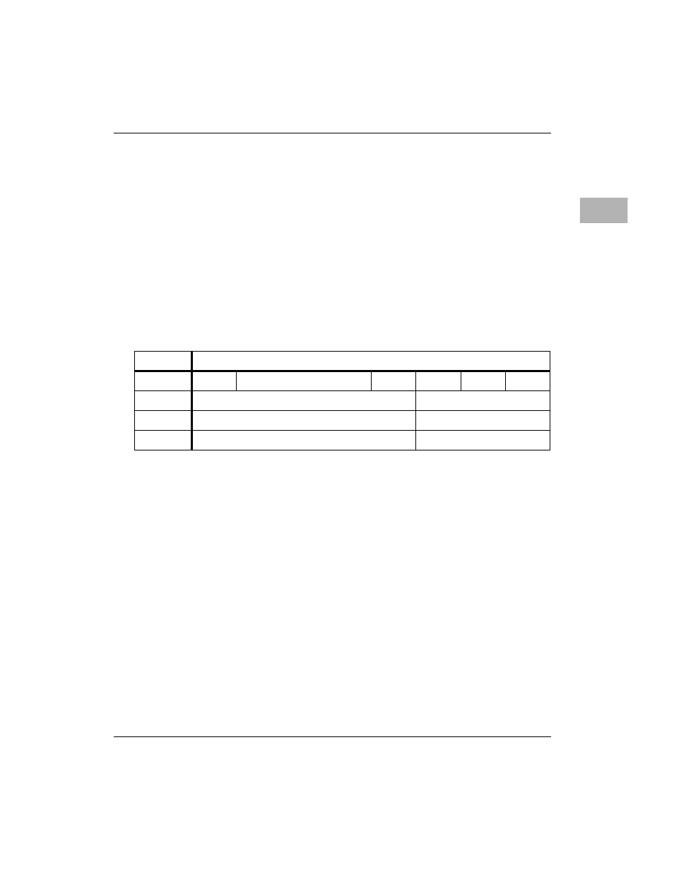
DRAM Space Base Address Register
B31-B20
B31 - B20 are compared to local bus address signals A31
- A20 for memory reference cycles. If they compare, a
DRAM cycle is initiated. Note that there is linkage
between the Base Address Register and its associated Size
Register. The Size Register masks the least significant
address signals for the comparison. Therefore, the Base
Address Register contents must be set to a multiple of the
Size Register. For example, if the size is set for 4096 KB,
the Base Register must be set to 0, or 4096 KB, or 8192
KB, or 12288 KB, etc.
ADR/SIZ
$FFF42020 (16 bits)
BIT
31
..
20
19
..
16
NAME
B31-B20
OPER
R/W
R
RESET
0 PL
0
