Motorola MVME172 User Manual
Page 301

Programming Model
http://www.mcg.mot.com/literature
5-11
5
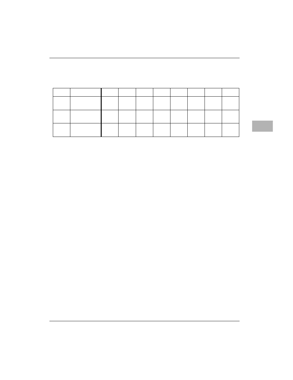
A summary of the remaining CSR registers is shown in
,
following. As with the first eight CSR registers, the summary shows the
registers for the upper MCECC. The registers for the lower MCECC
appear on D8-D15. As with the first eight CSR registers, software should
read and write to only the upper MCECC CSRs. The exception to this is
the error logger, error address, and error syndrome registers. These
registers contain information specific to each MCECC and the DRAMs
which it controls, and as such should be treated separately. The base
address of the CSRs is hard coded to the address $FFF43000 for the
MCECC pair on the first mezzanine board and $FFF43100 for the
MCECC pair on the second mezzanine board.
$10
DUMMY 1
0
0
0
0
0
0
0
0
$14
BASE
ADDRESS
BAD31
BAD30
BAD29
BAD28 BAD27
BAD26
BAD25
BAD24
$18
DRAM
CONTROL
BAD23
BAD22
BAD21
BAD20 BAD19
BAD18
BAD17
BAD16
$1C
BCLK
FREQUENCY
BCK7
BCK6
BCK5
BCK47
BCK3
BCK2
BCK1
BCK0
Table 5-2. MCECC Internal Register Memory Map, Part 1
MCECC Base Address = $FFF43000 (1st); $FFF43100 (2nd)
