Sram space base address register, Dram space size register – Motorola MVME172 User Manual
Page 214

3-26
Computer Group Literature Center Web Site
MC2 Chip
3
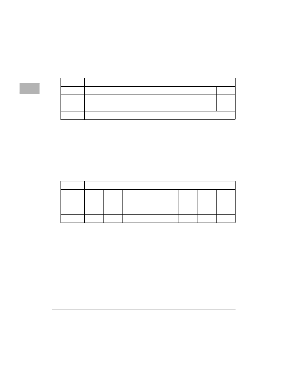
SRAM Space Base Address Register
B31-B17
B31 - B17 are compared to local bus address signals A31
- A17 for memory reference cycles. If they compare, an
SRAM cycle is initiated. Note that the same linkage that
exists between the DRAM Base and Size Registers also
exists for the SRAM decode logic. Refer to the DRAM
Space Base Register description.
DRAM Space Size Register
DZ2-DZ0 The size bits configure the non-ECC DRAM decoder for
a particular memory size. The following table defines
their encoding. Note that the table specifies the allowed
bit combinations for DZ2 - DZ0. Any other combinations
generate unpredictable results.
DZ2 - DZ0 are set equal to the DZ2 - DZ0 bits of the
DRAM/SRAM Options Register. Note that changing DZ2
- DZ0 so that the DRAM architecture changes between
interleaved and non-interleaved relocates the data. DZ2 -
DZ0 are programmable to facilitate diagnostic software.
ADR/SIZ
$FFF42020 (16 bits)
BIT
15-1
0
NAME
B31-B17
OPER
R/W
R
RESET
$FFE0 PL
ADR/SIZ
$FFF42024 (8 bits)
BIT
31
30
29
28
27
26
25
24
NAME
DZ2
DZ1
DZ0
OPER
R/W
R/W
R/W
R/W
R/W
R/W
R/W
R/W
RESET
0 PL
0 PL
0 PL
0 PL
0 PL
0 PL
0 PL
0 PL
