Dram control register, Dram control register -18, 5dram control register – Motorola MVME172 User Manual
Page 308
5-18
Computer Group Literature Center Web Site
MCECC
5
DRAM Control Register
The bit assignments for the DRAM Control Register are:
RAMEN
RAM Enable. This control bit is used to enable the local
bus to perform read/write accesses to the memory.
Accesses are enabled when this bit is set and are disabled
when this bit is cleared. This bit should only be set after
BAD31-BAD22 have been initialized.
Difference from MEMC040: none.
NCEBEN Setting the NCEBEN control bit enables the MCECC pair
to assert TEA* when a non-correctable error occurs
during a local bus access to memory. In some cases setting
NCEBEN causes DRAM accesses to be delayed by one
clock. This delay is incurred when the access is a local bus
(or scrub) read and the FSTRD bit is set.
Difference from MEMC040: bit = PAREN for
MEMC040; bit = NCEBEN for MCECC (both accomplish
basically the same thing, enabling TEA assertion for non-
correctable errors).
NCEIEN
When NCEIEN is set, the logging of a non-correctable
error causes the INT signal pin to pulse true. Note that
NCEIEN has no effect on DRAM access time.
Difference from MEMC040: bit = PARINT for
MEMC040; bit = NCEIEN for MCECC.
RWB3
Read/Write Bit 3 is a general purpose read/write bit
ADR/SIZ
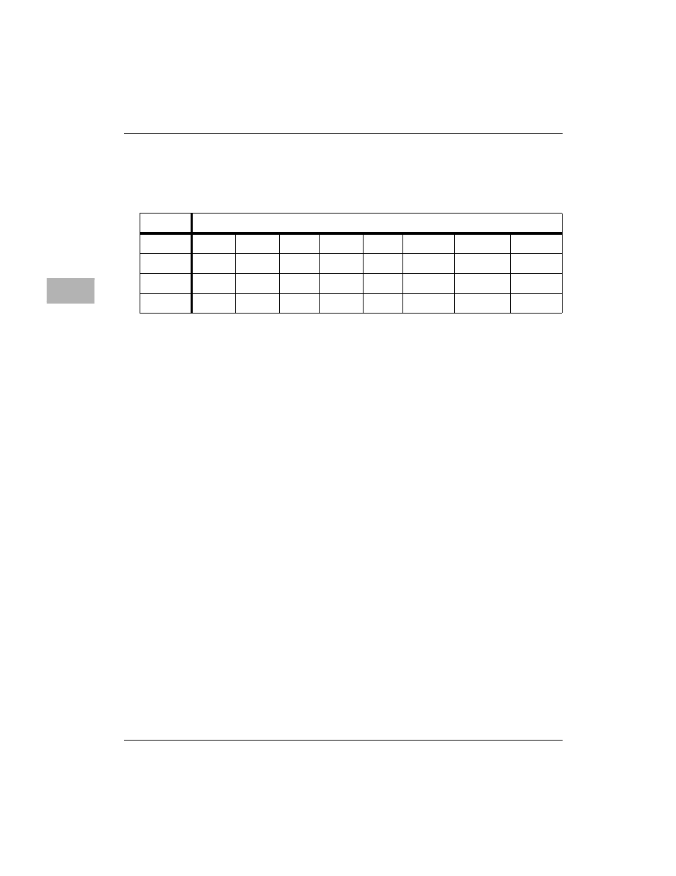
1st $FFF43018/2nd $FFF43118 (8-bits)
BIT
31
30
29
28
27
26
25
24
NAME
BAD23 BAD22 RWB5 SWAIT
RWB3 NCEIEN
NCEBEN
RAMEN
OPER
R/W
R/W
R/W
R/W
R/W
R/W
R
R/W
RESET
0 PLS
0 PLS
0 PLS
0 PLS
0 PLS
0 PLS
0 PLS
0 PLS