Flash access time control register, Flash access time control register -40 – Motorola MVME172 User Manual
Page 228
3-40
Computer Group Literature Center Web Site
MC2 Chip
3
ROM0
Refer to the table on the Local Bus Memory Map, Note 1,
in Chapter 1.
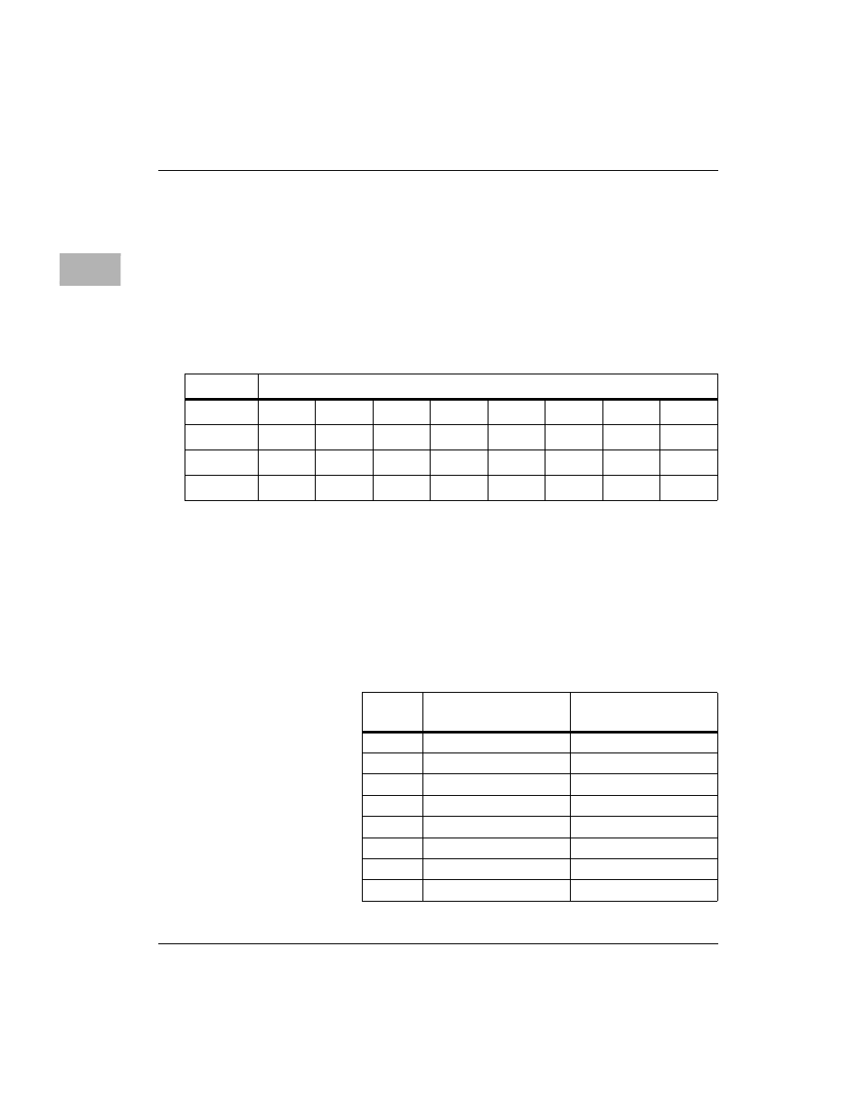
Flash Access Time Control Register
The MVME172 is populated with a 120ns Flash memory device. Due to
the wide range of Flash speeds, the contents can be changed by software to
adjust for a specific speed.
FWEN
Flash write enable function is internal to the ASIC for the
MC2 chip. FWEN set to a 1 enables writes to the Flash
memory space. FWEN set to a 0 inhibits writes to the
Flash memory but the cycle completes without exception.
FT2-FT0
Flash memory access time is controlled by the state of
FT2-FT0. The following table defines the FT2-FT0
encoding (for the MVE172, whose bus frequency is
1
/
2
the
processor frequency, only the 33MHz column applies).
ADR/SIZ
$FFF42040 (8 bits)
BIT
15
14
13
12
11
10
9
8
NAME
FWEN
FT2
FT1
FT0
OPER
R
R
R
R
R/W
R/W
R/W
R/W
RESET
0
0
0
0
0
1 PL
1 PL
1 PL
FT2-
FT0
Flash Access <= N
at 25 MHz where N =
Flash Access <= N
at 33 MHz where N =
$0
60 ns
40 ns
$1
100 ns
70 ns
$2
140 ns
100 ns
$3
180 ns
130 ns
$4
220 ns
160 ns
$5
260 ns
190 ns
$6
300 ns
210 ns
$7
340 ns
240 ns