Dummy register 0, Dummy register 0 -16 – Motorola MVME172 User Manual
Page 306

5-16
Computer Group Literature Center Web Site
MCECC
5
RB3
Read Bit 3 is a read only bit that is always 0.
Difference from MEMC040: bit = WPB (write-per-bit
input strap status) for MEMC040; bit = 0 for MCECC
(WPB = 0 on current versions of MVME172).
RB4
Read Bit 4 is a read only bit that is always 1.
Difference from MEMC040: bit = EXTPEN (external
parity enable input strap status) for MEMC040; bit = 1 for
MCECC (EXTPEN = 1 on current versions of
MVME172).
FSTRD
FSTRD reflects the state of the FSTRD bit in the Defaults
Register 1. When 1, this bit indicates that DRAM reads
are operating at full speed. When 0, it indicates that
DRAM read accesses are slowed by one clock cycle to
accommodate slower DRAM devices.
Difference from MEMC040: NONE except that it is an
input pin on the MEMC040; while it is a register bit that
is initialized by the reset serial bit stream on the MCECC.
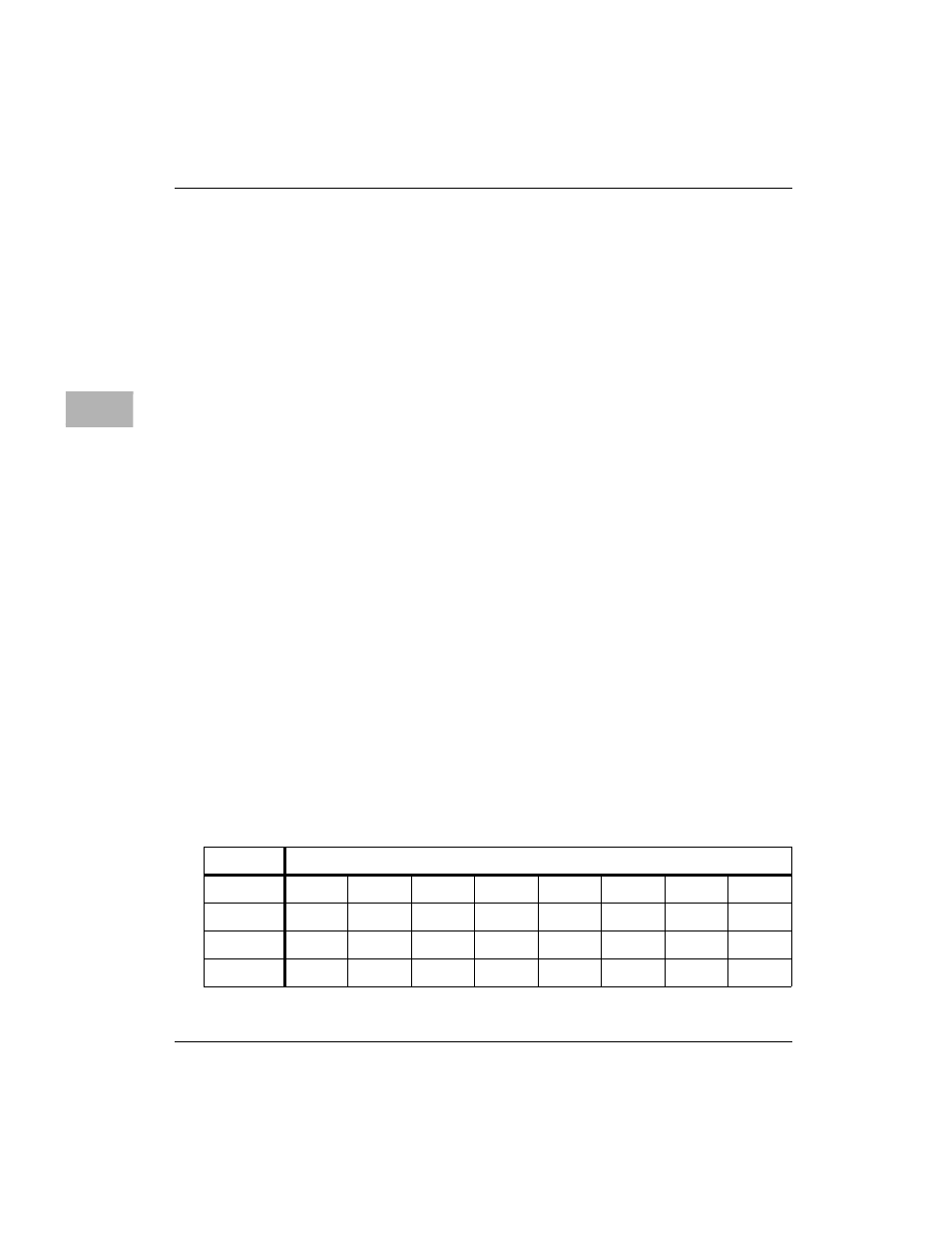
Dummy Register 0
Dummy Register 0 is hard-wired to all zeros. Writes to this register are
ignored; however, the MCECC always terminates the cycles properly with
TA*.
Difference from MEMC040: register = Alternate Status
for MEMC040; register = $00 for MCECC.
ADR/SIZ
1st $FFF4300C/2nd $FFF4310C (8-bits)
BIT
31
30
29
28
27
26
25
24
NAME
0
0
0
0
0
0
0
0
OPER
R
R
R
R
R
R
R
R
RESET
X
X
X
X
X
X
X
X
