Bclk frequency register, Bclk frequency register -20 – Motorola MVME172 User Manual
Page 310

5-20
Computer Group Literature Center Web Site
MCECC
5
Difference from MEMC040: bit = DMCTL (data-mux-
control) for MEMC040; bit = RWB (general purpose read
write bit) for MCECC (data-mux-control not required for
MCECC pair).
BAD22, BAD23
These are the lower two bits of the DRAM base address
described in the previous register.
Difference from MEMC040: none.
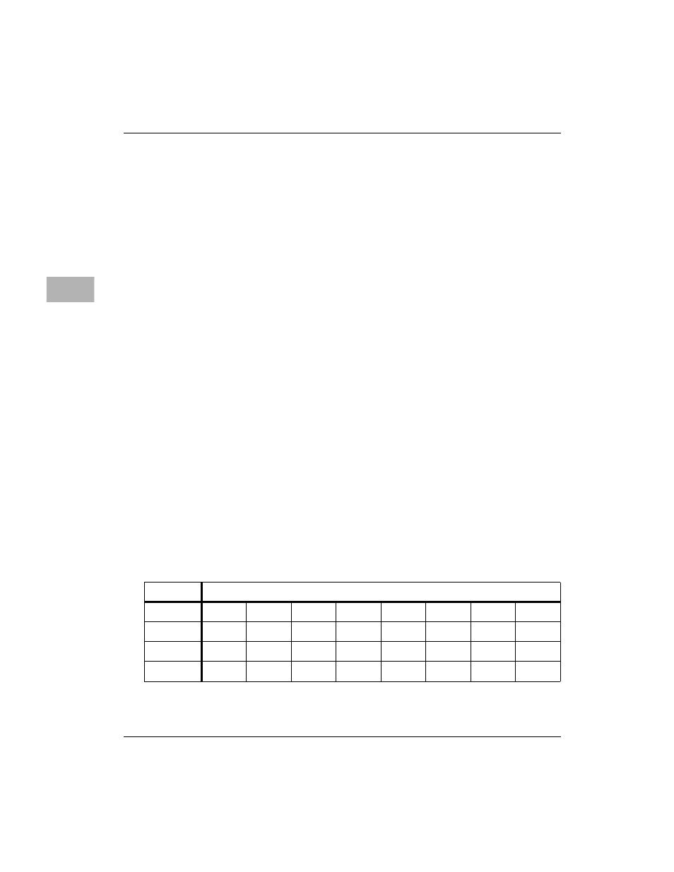
BCLK Frequency Register
The Bus Clock (BCLK) Frequency Register should be programmed with
the hexadecimal value of the operating clock frequency in MHz (i.e., $19
for 25 MHz and $21 for 33 MHz). The MCECC pair uses the value
programmed in this register to control the Prescaler Counter. The Prescaler
Counter increments to $FF and then it is loaded with the two’s compliment
of the value in the BCLK Frequency Register. This produces a 1 MHz
clock that is used by the refresh timer and the scrubber. When the BCLK
Frequency Register is correctly programmed with the BCLK frequency,
the DRAMs are refreshed approximately once every 15.6 microseconds.
After power-up, this register is initialized to $19 (for 25 MHz).
Difference from MEMC040: none.
Note
This register is configured only during power-up-reset and is
unchanged by software or local reset.
ADR/SIZ
1st $FFF4301C/2nd $FFF4311C (8-bits)
BIT
31
30
29
28
27
26
25
24
NAME
BCK7
BCK6
BCK5
BCK4
BCK3
BCK2
BCK1
BCK0
OPER
R/W
R/W
R/W
R/W
R/W
R/W
R/W
R/W
RESET
0 P
0 P
0 P
1 P
1 P
0 P
0 P
1P
