I/o control register 1, I/o control register 1 -97 – Motorola MVME172 User Manual
Page 175
LCSR Programming Model
http://www.mcg.mot.com/literature
2-97
2
I/O Control Register 1
This register is a general purpose I/O control register. Bits 16-19 control
the direction of the four General Purpose I/O pins (GPIO0-3).
GPOEN0
When this bit is low, the GPIO0 pin is an input.
When this bit is high, the BPIO0 pin is an output.
GPOEN1
When this bit is low, the GPIO1 pin is an input.
When this bit is high, the BPIO1 pin is an output.
GPOEN2
When this bit is low, the GPIO2 pin is an input.
When this bit is high, the BPIO2 pin is an output.
GPOEN3
When this bit is low, the GPIO3 pin is an input.
When this bit is high, the BPIO3 pin is an output.
ABRTL
This bit indicates the status of the
ABORT
switch.
When this bit is high, the
ABORT
switch is depressed.
When this bit is low, the
ABORT
switch is not depressed.
ACFL
This bit indicates the status of the ACFAIL signal line on
the VMEbus. When this bit is high, the ACFAIL signal
line is active. When this bit is low, the ACFAIL signal line
is not active.
SYSFL
This bit indicates the status of the SYSFAIL signal line on
the VMEbus. When this bit is high, the SYSFAIL signal
line is active. When this bit is low, the SYSFAIL signal
line is not active.
MIEN
When this bit is low, all interrupts controlled by the
VMEchip2 are masked. When this bit is high, all
interrupts controlled by the VMEchip2 are not masked.
ADR/SIZ
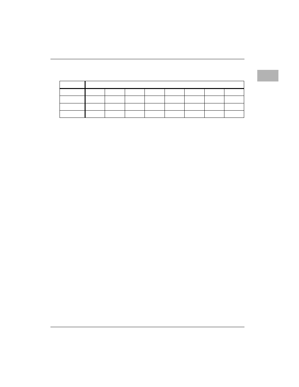
$FFF40088 (8 bits of 32)
BIT
23
22
21
20
19
18
17
16
NAME
MIEN
SYSFL
ACFL
ABRTL
GPOEN3 GPOEN2 GPOEN1 GPOEN0
OPER
R/W
R
R
R
R/W
R/W
R/W
R/W
RESET
0 PSL
X
X
X
0 PS
0 PS
0 PS
0 PS