Motorola MVME172 User Manual
Page 26
1-8
Computer Group Literature Center Web Site
Board Description and Memory Maps
1
Notes
1.
RESET
switch control.
2. Watchdog timer control.
3. Access and watchdog timer parameters.
4. MPU TEA (bus error) status
5. Bit numbering for VMEchip2 and MC2 chip has a one-to-
one correspondence.
6.
ABORT
switch interrupt control. Implemented also in the
VMEchip2, but with a different bit organization (refer to the
VMEchip2 description in Chapter 2). In the MVME172, the
ABORT
switch is wired to the MC2 chip, not the VMEchip2.
7. The SRAM and PROM decoder in the VMEchip2 (version
2) must be disabled by software before any accesses are made
to these address spaces.
8. 32-bit prescaler. The prescaler can also be accessed at
$FFF40064 when the optional VMEbus is not enabled.
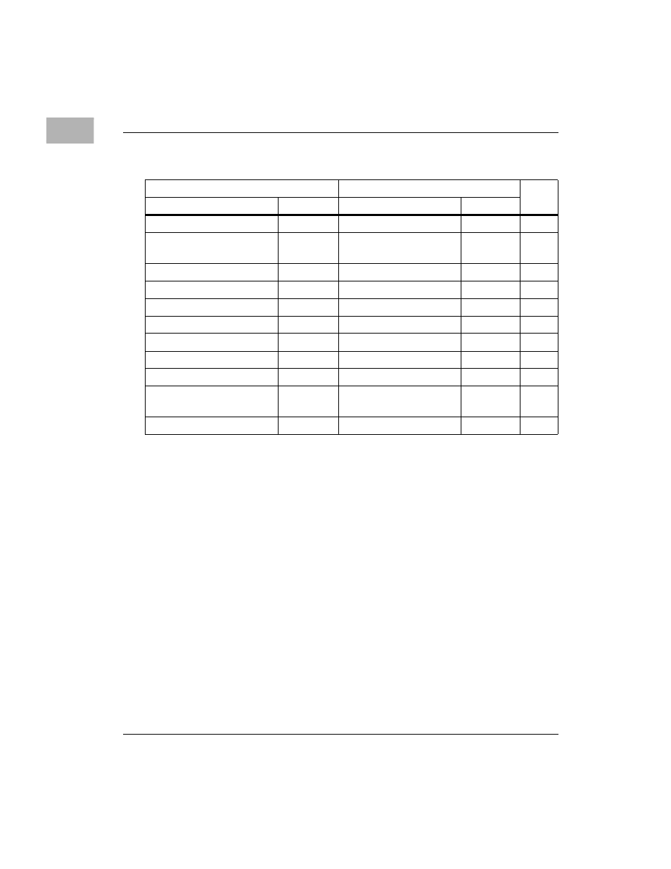
Table 1-2. Redundant Functions in the VMEchip2 and MC2 Chip
VMEchip2
MC2 Chip
Notes
Address
Bit #
Address
Bit #
$FFF40060
28 - 24
$FFF42044
28 - 24
1,5
$FFF40060
22 -
19,17,16
$FFF42044
22 -
19,17,16
2,5
$FFF4004C
13 - 8
$FFF42044
13 - 8
3,5
$FFF40048
7
$FFF42048
8
4
$FFF40048
9
$FFF42048
9
4,5
$FFF40048
10
$FFF42048
10
4,5
$FFF40048
11
$FFF42048
11
4,5
$FFF40064
31 - 0
$FFF4204C
31 - 0
8
$FFF42040
6 - 0
6
$FF800000-$FFBFFFFF
31 - 0
$FF800000-
$FFBFFFFF
31 - 0
7
$FFE00000-$FFEFFFFF
31 - 0
Programmable
31 - 0
7