Dram control register, Dram control register -45 – Motorola MVME172 User Manual
Page 233

Programming Model
http://www.mcg.mot.com/literature
3-45
3
signal is sent to the local bus. Note that the Version
Register bit V1 must be set to a 1 to enable the MC2 chip
access timer (i.e., it must be a "No VMEbus Interface"
option).
0
8
µ
s
1
64
µ
s
2
256
µ
s
3
The timer is disabled.
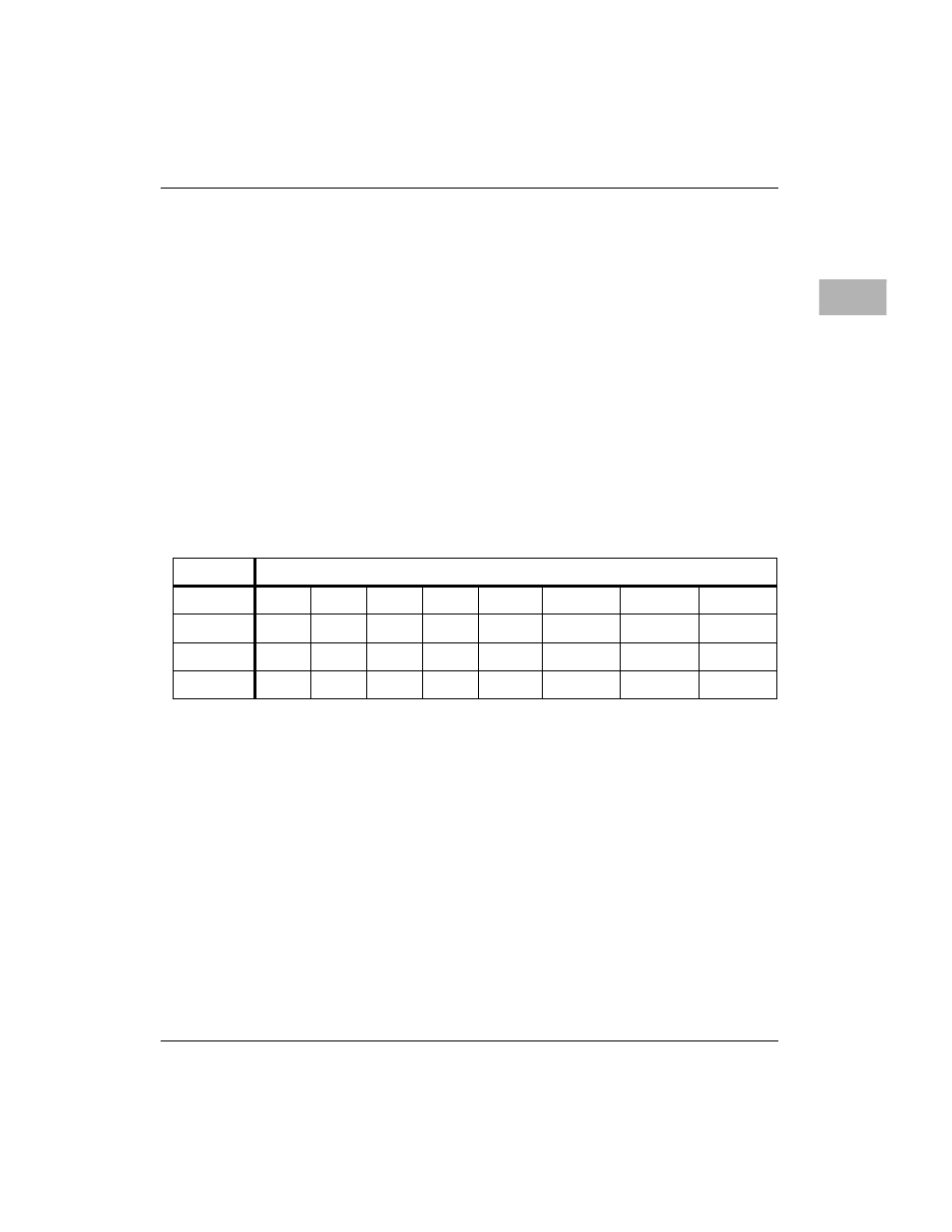
DRAM Control Register
This register controls the parity checking mode and DRAM enable for
non-ECC applications.
RAMEN
This bit enables the access of the DRAM. The DRAM
should be enabled after the DRAM Space Base Address
Register is enabled and the ROM0 bit has been cleared.
The DRAM Space Base Address Register is located at
$FFF42020 bits 31 - 16 and the ROM0 bit is located at
$FFF42040 bit 20.
ADR/SIZ
$FFF42048 (8 bits)
BIT
31
30
29
28
27
26
25
24
NAME
WWP
PARINT
PAREN
RAMEN
OPER
R/W
R/W
R/W
R/W
R/W
R/W
R/W
R/W
RESET
0
0
0
0
0 PL
0 PL
0 PL
0 PL
- SB5101U DOCSIS 2.0 Cable Modem (16 pages)
- PTP 500 (20 pages)
- Netopia 3347-02-ENT (3 pages)
- SBV5220 (64 pages)
- AP-51XX (698 pages)
- SURFboard SVG2501 Series (34 pages)
- MESH Wireless Router MWR6300 (2 pages)
- MVME712AM (74 pages)
- SURFBOARD SBG1000 (16 pages)
- RSGu3502 (5 pages)
- SURFboard SBG941U (78 pages)
- Netopia 2240N-VGx (5 pages)
- SURFboard SVG2501 (8 pages)
- WR850GP (95 pages)
- WR850G (93 pages)
- USBW 200 (12 pages)
- ONCE SC140 (28 pages)
- Netopia 3300 (368 pages)
- MPC8260 (1006 pages)
- WNS25 (2 pages)
- Netopia 7000 (254 pages)
- Viadux 2000 Subscriber Bridge RC2010 (1 page)
- MVME5100 Series (5 pages)
- ColdFire MCF5282 (766 pages)
- MC9S12C-Family (136 pages)
- CG4500 (36 pages)
- SBG900 (130 pages)
- SURFBOARD SB5100 (2 pages)
- SURFboard SB6180 (20 pages)
- SURFBOARD SBG900 (16 pages)
- SURFboard SVG1501U (83 pages)
- SB5100 (74 pages)
- T3 (2 pages)
- H375 (5 pages)
- NETOPIA 2247/57-62 (22 pages)
- SBV5120 (56 pages)
- SBV5120 (57 pages)
- RG2200 (88 pages)
- CME-12B/BC (18 pages)
- SURFboard 574823-001-a (2 pages)
- SURFboard Cable Modem (66 pages)
- CME-12D60 (19 pages)
- DIGITAL VOICE MODEM SBV5122 (24 pages)
- SB4000 (2 pages)
- Canopy FSK and OFDM radios PTP 200 (OFDM (56 pages)
