Watchdog timer control register, Watchdog timer control register -43, 3watchdog timer control register – Motorola MVME172 User Manual
Page 231

Programming Model
http://www.mcg.mot.com/literature
3-43
3
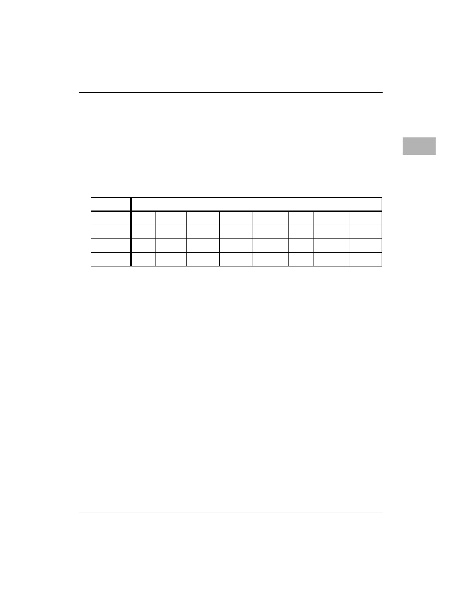
Watchdog Timer Control Register
The watchdog timer control logic in the MC2 chip is used with the "No
VMEbus Interface" option. This function is duplicated at the same bit
locations in the VMEchip2 at location $FFF40060. The VMEchip2 has the
additional option of selecting SYSRESET (i.e., VMEbus reset). It is
permissible to enable the watchdog timer in both the VMEchip2 and the
MC2 chip.
WDEN
When this bit is high, the watchdog timer is enabled.
When this bit is low, the watchdog timer is not enabled.
WDRSE
When this bit is high, and a watchdog time-out occurs, a
LRESET is generated. When this bit is low, a watchdog
time-out does not cause a reset.
WDBFE
When this bit is high and the watchdog timer has timed
out, the MC2 chip asserts the BRDFAIL signal pin. When
this bit is low, the watchdog timer does not contribute to
the BRDFAIL signal on the MC2 chip.
WDTO
When this status bit is high, a watchdog time-out has
occurred. When this status bit is low, a watchdog time-out
has not occurred. This bit is cleared by writing a one to the
WDCS bit in this register.
WDCC
When this bit is set high, the watchdog counter is reset.
The counter must be reset within the time-out period or a
watchdog time-out occurs.
WDCS
When this bit is set high, the watchdog time-out status bit
(WDTO bit in this register) is cleared.
ADR/SIZ
$FFF42044 (8 bits)
BIT
23
22
21
20
19
18
17
16
NAME
WDCS
WDCC
WDTO
WDBFE
WDRSE
WDEN
OPER
R
C
C
R
R/W
R
R/W
R/W
RESET
0
0 P
0 P
0 P
0 PL
0
0 PL
0 PL
