Data control register – Motorola MVME172 User Manual
Page 311

Programming Model
http://www.mcg.mot.com/literature
5-21
5
Note
None of the remaining registers have counterparts in the
MEMC040 because they are associated with functions
contained only in the MCECC pair.
Data Control Register
RWCKB
READ/WRITE CHECKBITS, when set, enables the data
from the eight checkbits in this MCECC to be written and
read on the local MC68060 data bus (bits 24-31 for upper
MCECC, bits 8-15 for lower MCECC). This bit should be
cleared for normal system operation. Note that if test
software forces a single bit error to a location (line) using
this function, the scrubber may correct the location before
the test software gets a chance to check for the single bit
error at that location. This can be avoided by disabling
scrubbing and making sure that all previous scrubs have
completed, before performing the test. Also note that
writing bad checkbits can set the ERRLOG bit in the Error
Logger Register.
The writing of checkbits causes the MCECC to perform a
read-modify-write to DRAM. If the location to which
check bits are being written, has a single or double bit err,
data in the location may be altered by the write checkbits
operation. To avoid this, it is recommended that the
DERC bit also be set while the RWCKB bit is set. A
suggested sequence for performing read-write checkbits
is as follows:
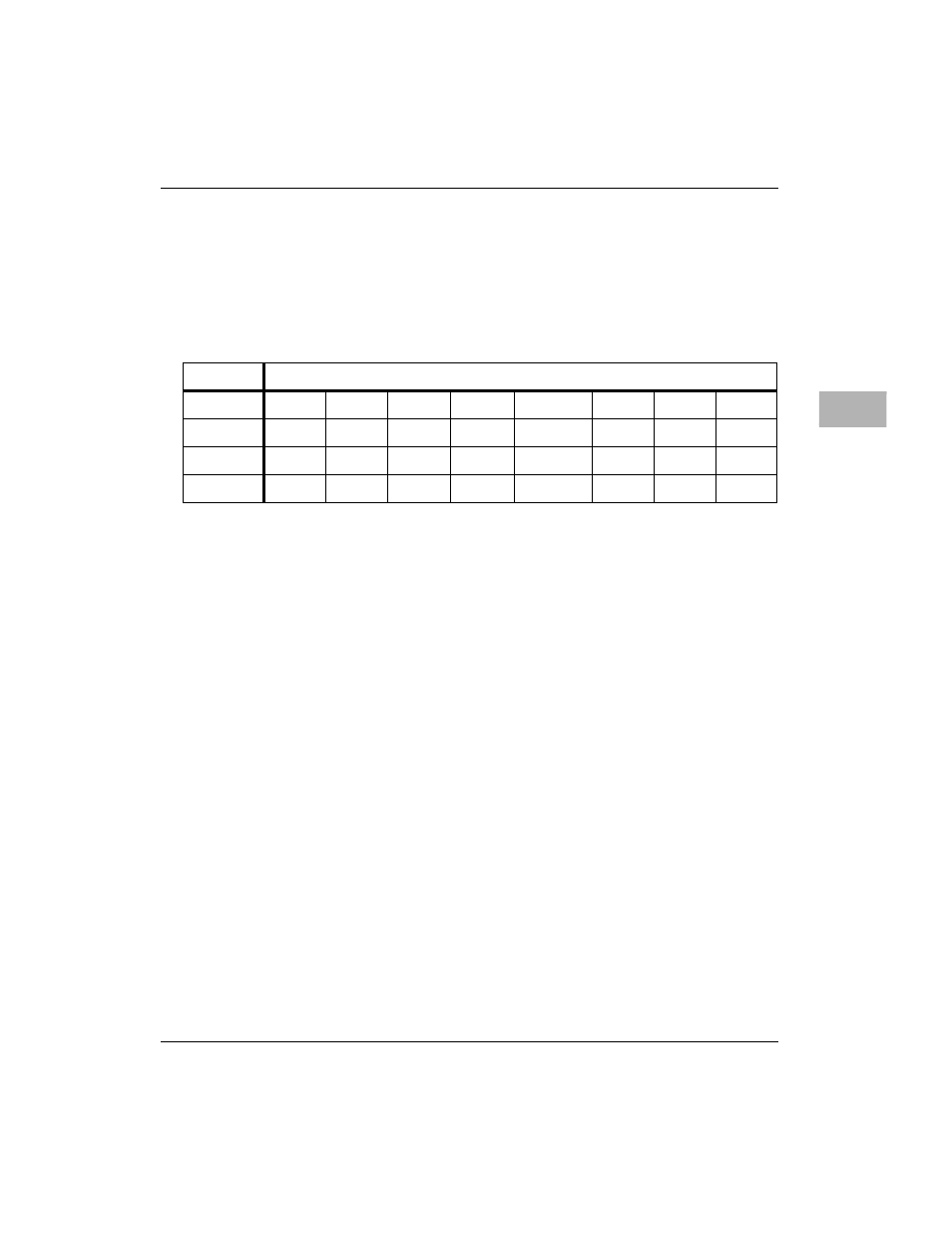
ADR/SIZ
1st $FFF43020/2nd $FFF43120 (16-bits)
BIT
31
30
29
28
27
26
25
24
NAME
0
0
DERC
ZFILL
RWCKB
0
0
0
OPER
R
R
R/W
R/W
R/W
R
R
R
RESET
X
X
1 PLS
0 PLS
0 PLS
X
X
X
