Vector base register, Vector base register -18, 4vector base register – Motorola MVME172 User Manual
Page 254
4-18
Computer Group Literature Center Web Site
IP2 Chip
4
Vector Base Register
The interrupt Vector Base Register is an 8-bit read/write register that is
used to supply the vector to the CPU during an interrupt acknowledge
cycle for the four DMA controller interrupts and for the programmable
clock interrupt. Only the most significant five bits are used. The least
significant three bits encode the interrupt source during the acknowledge
cycle. The exception to this is that after reset occurs, the interrupt vector
passed is $07, which remains in effect until a write is generated to the
Vector Base Register.
Note
Note that this register does not affect the vector supplied
during an interrupt acknowledge cycle for any of the eight
IndustryPack IRQ*s.
!
Caution
For some versions of the IP2 chip, this register is write only.
There is NO known workaround for this error. This register
does return the correct value for the interrupt acknowledge
cycle.
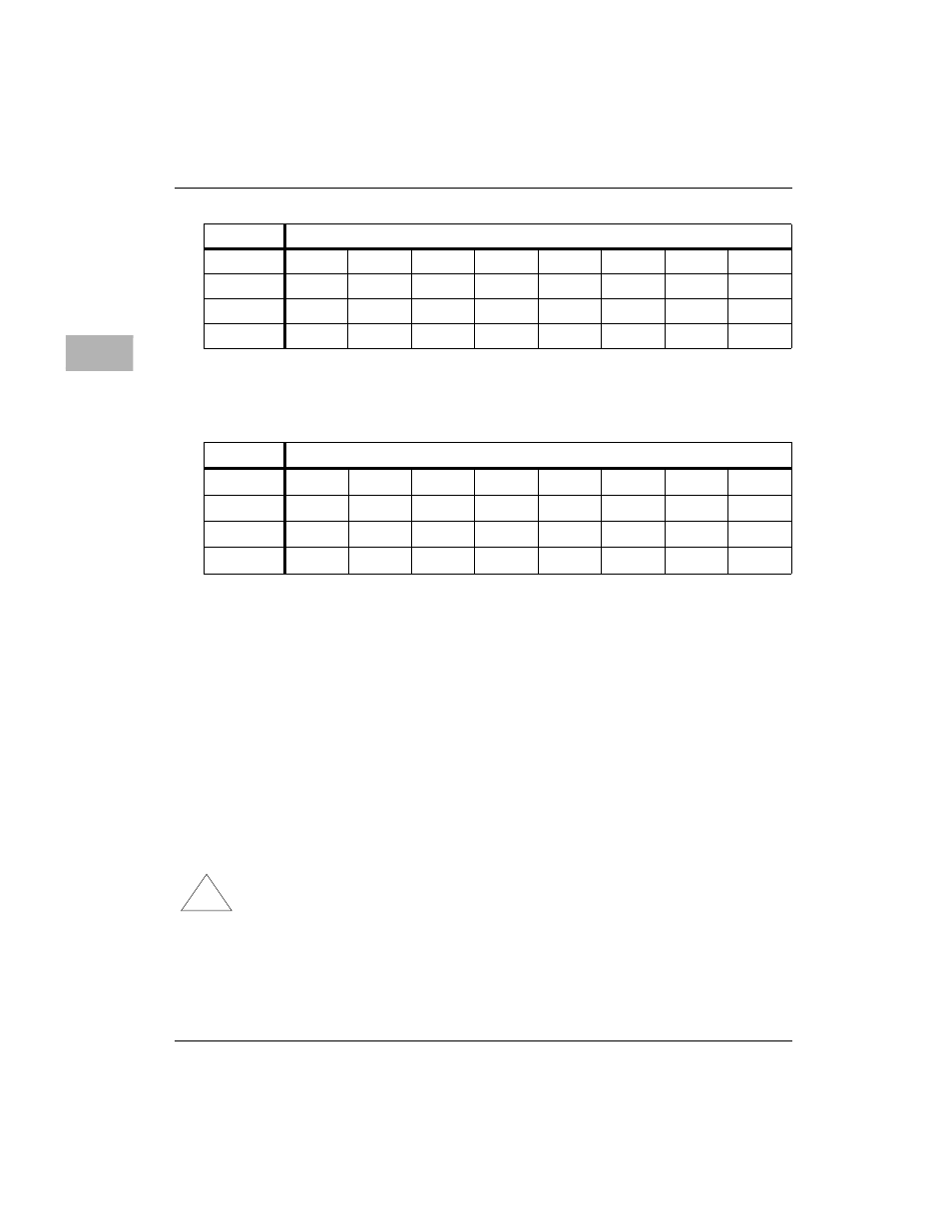
ADR/SIZ
$FFFBC001 (8 bits)
BIT
7
6
5
4
3
2
1
0
NAME
REV7
REV6
REV5
REV4
REV3
REV2
REV1
REV0
OPER
R
R
R
R
R
R
R
R
RESET
0
0
0
0
0
0
0
1
ADR/SIZ
$FFFBC003 (8 bits)
BIT
7
6
5
4
3
2
1
0
NAME
IV7
IV6
IV5
IV4
IV3
IV2
IV1
IV0
OPER
R/W
R/W
R/W
R/W
R/W
R
R
R
RESET
0
0
0
0
1
1
1
1