Table 46, 7 option card installation, Complementary output – Yaskawa CIMR-LU Drives User Manual
Page 152: Open-collector outputs
7 Option Card Installation
152
YASKAWA ELECTRIC TOEP C710616 38F YASKAWA AC Drive L1000A Quick Start Guide
Take the following steps to prevent erroneous operation caused by noise interference:
• Use shielded wire for the PG encoder signal lines.
• Limit the length of all motor output power cables to less than 100 m. Limit the length of open-collector output lines to
less than 50 m.
• Use separate conduit or cable tray dividers to separate option control wiring, main circuit input power wiring, and
motor output power cables.
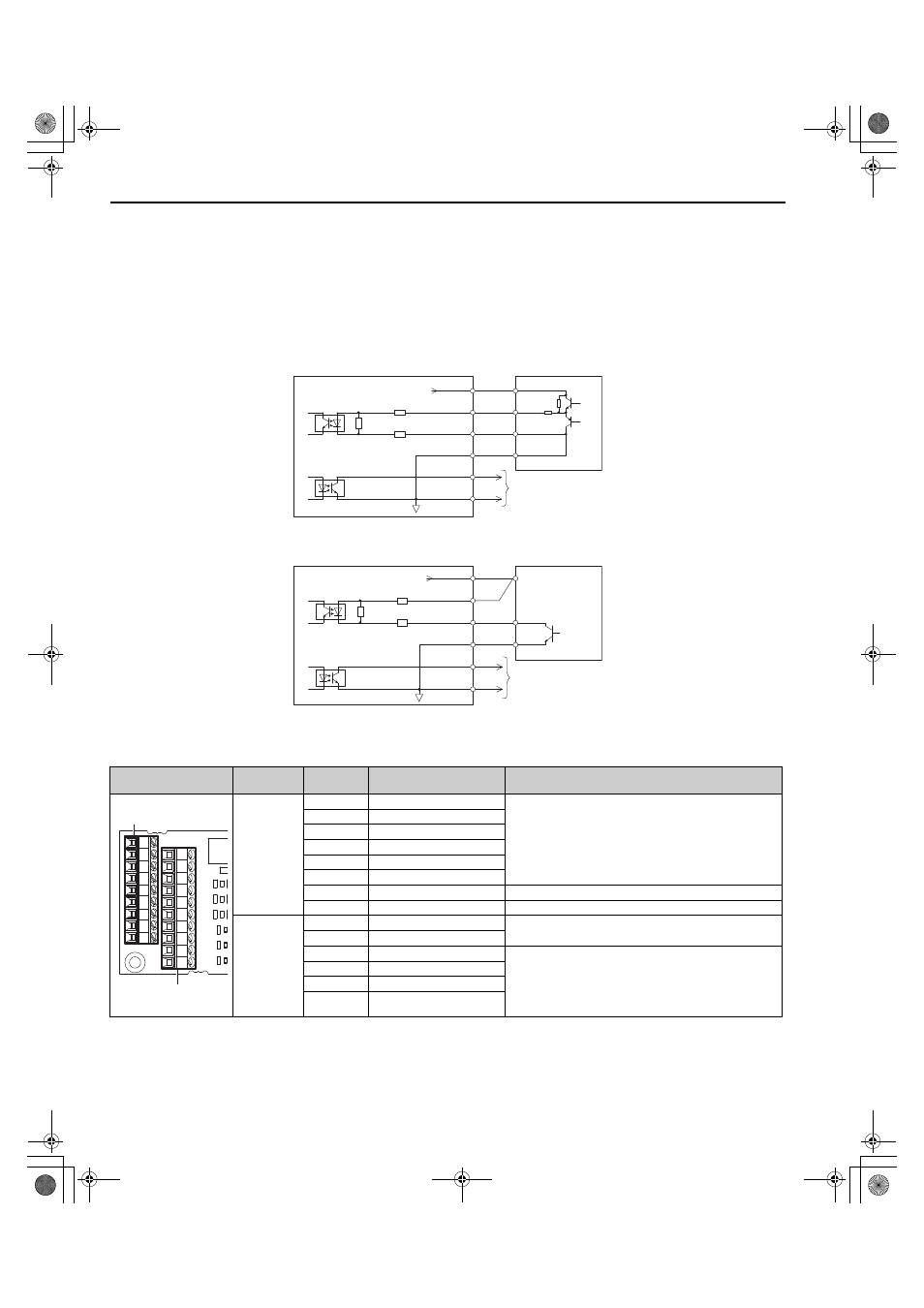
Interface Circuit
• Complementary Output
Figure 84
Figure 92 Complementary Outputs for the Interface Circuit
• Open-Collector Outputs
Figure 85
Figure 93 Open-Collector Outputs for the Interface Circuit
Terminal Functions
Table 46 Option Terminal Functions
Terminal
Block
Terminal
Function
Description
TB1
<1> A separate UL-listed class 2 power supply is necessary when the PG requires more than 200 mA to operate.
A+
A+ pulse signal input
• Pulse signal inputs from the PG.
• Signal inputs from complementary and open-collector
outputs
• Signal level
H level: 8 to 12 V
L level: 2.0 V or less
A–
A– pulse signal input
B+
B+ pulse signal input
B–
B– pulse signal input
Z+
Z+ pulse signal input
Z–
Z– pulse signal input
SD
NC pin (open)
For use when cables shields should not be grounded
FE
Ground
Used for grounding shielded lines
TB2
IP
PG power supply
• Output voltage: 12.0 V ± 5%
• Max output current: 200 mA
IG
PG power supply common
AO
A pulse monitor signal
• Outputs the monitor signal for the A, B, and Z pulses
from the PG speed control card
• For open collector outputs from the option
• Max voltage: 24 V
• Max current: 30 mA
BO
B pulse monitor signal
ZO
Z pulse monitor signal
IG
Monitor signal common
PG-B3
PG Encoder
470
Ω
330
Ω
330
Ω
A-,B-,Z-
A+,B+,Z+
IG
AO,BO,ZO
0V
A,B,Z
Vcc
IP
IG
0V
12 V
Monitor Signals
PG
B3
470
Ω
330
Ω
330
Ω
A+,B+,Z+
IG
AO,BO,ZO
IP
IG
12 V
PG Encoder
A,B,Z
Vcc
0V
A
,B,Z
Monitor Signals
AO
IG
IG
ZO
IG
BO
IG
IP
A-
A+
FE
SD
Z-
Z+
B-
B+
TB1
TB2
TOEP_C710616_38F_5_0.book 152 ページ 2013年12月4日 水曜日 午前9時56分