Input/output controller hub 2 (82801ba), Figure28 system block diagram using ich2, Figure 2-8 system block diagram using ich2 – HP A7818-IE002 User Manual
Page 44
System Board
Input/output Controller Hub 2 (82801BA)
Chapter 2
44
Input/output Controller Hub 2 (82801BA)
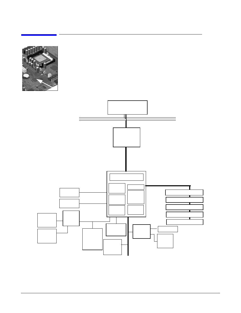
The ICH2 is encapsulated in a 360-pin Enhanced Ball Grid Array (EBGA) package and
resides on the system board just underneath the AGP connector. It provides the interface
between the PCI bridge (PCI 2.2 compliant with support for 32-bit 33MHz PCI
operations),
PCI-to-Low Pin Count (LPC) bridge, IDE controller, USB controller, SMBus controller,
and Audio Codec’97 controller.
You’ll find more detail about the ICH2 functions and capabilities later in this section.
Figure 2-8 shows an example of the system block diagram using the ICH2.
Figure 2-8
System Block Diagram Using ICH2
LPC/FWH link
I850 Memory
Controller Hub
(MCH)
MaxiLife
Monitor-
ing Chip
Serial
EEPROM
SMBus
Address (36)
Control
Data (64)
ATA/100 2
channels
4 x USB
Controller
LCD
Status
Panel
Parallel
and serial
ports
Keyboard,
mouse,
and floppy
System Bus
2 IDE
connectors
4 USB
connectors
FirmWare
Hub
(FWH)
82802AA
USB
Super
I/O
NS 87364
SM Bus
Controller
Fans
Intel Pentium IV
Processor
I/O Controller Hub
(ICH2) 82801BA
PCI Bridge
IDE
Control
ler
DMA
Controller
CS audio
codec
(CS4280)
Slot 1 - 32-bit/33MHz
Slot 2- 32-bit/33MHz
Slot 3 - 32-bit/33MHz
PCI bus (32-bit, 33MHz)
133MB/s data transfer rate
Slot 4 - 32-bit/33MHz
Slot 5 - 32-bit/33MHz
Lan
Interface