Memory controller hub (82850), Figure26 system block diagram using mch – HP A7818-IE002 User Manual
Page 38
System Board
Memory Controller Hub (82850)
Chapter 2
38
Memory Controller Hub (82850)
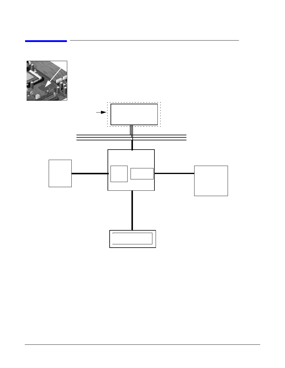
The MCH host bridge/controller is contained in a 615-pin Organic Land Grid Array
(OLGA) package and is the bridge between the system bus, Dual Rambus bus (main
memory), AGP 4x (graphic), and Hub Link 8-bit.
Figure 2-6 shows an example of the system block diagram using the MCH.
Figure 2-6
System Block Diagram using MCH
I850 Memory
Controller Hub (MCH)
82850
Dual Rambus
Address (36)
Control
Data (64)
AGP 4x Bus
133MHz (1 GB
MB/s data transfer
rate)
HUB LINK 8
(266MB/s data
transfer rate)
I/O Controller Hub2
(ICH2) 82801BA
3.2GB/s at 400MHz
data transfer rate
AGP
Inter-
face
Memory
Controller
1.5V
AGP
PRO
connector
Socket 423
Intel Pentium IV
Processor
Four onboard
RIMM sockets
supporting
RDRAM
memory
100MHz two-way system bus
(Data Bus runs at 4 x 100MHz,
3.2GB/s transfer rate)
- UX B6941-90001 (548 pages)
- A3661B (95 pages)
- C100/110 (252 pages)
- L1702 (45 pages)
- 576X-B (1 page)
- rx5670 (13 pages)
- ProLiant PC2-6400 (38 pages)
- PC (120 pages)
- S3240 (2 pages)
- LC 2000R (194 pages)
- GS80 (41 pages)
- COMPAQ DX2710 MT (107 pages)
- TOUCHSMART 9100 (62 pages)
- BC1500 (13 pages)
- Proliant DL580 (48 pages)
- Proliant DL580 (53 pages)
- DX2200 (31 pages)
- ProLiant Server Blade BL460c (31 pages)
- P6000 (105 pages)
- d530 Series (2 pages)
- dc5700 (216 pages)
- RX7620-16 (43 pages)
- ProLiant ML370 G5 (46 pages)
- PROLIANT ML350 G6 (54 pages)
- BL35P (22 pages)
- COMPAQ DC5750 (214 pages)
- Agent-Desktop-Laptop Computer (23 pages)
- DL380 G7 (126 pages)
- xw8600 (73 pages)
- Pavilion A6140 (2 pages)
- Z800 (55 pages)
- 8080 ELITE BUSINESS (284 pages)
- VECTRA VL800 (72 pages)
- Vectra XE320 (82 pages)
- Vectra XE320 (32 pages)
- AA-RTDRB-TE (146 pages)
- BL465C (66 pages)
- DM4 (113 pages)
- PROLIANT 580554-001 (87 pages)
- ProLiant ML330 (34 pages)
- ProLiant ML330 (44 pages)
- PROLIANT BL465C G7 (30 pages)
- LH 3r (23 pages)
- Compaq dc7900 (3 pages)
- T5000 (41 pages)