Serial data signals – Altera Stratix V Avalon-MM Interface for PCIe Solutions User Manual
Page 60
Serial Data Signals
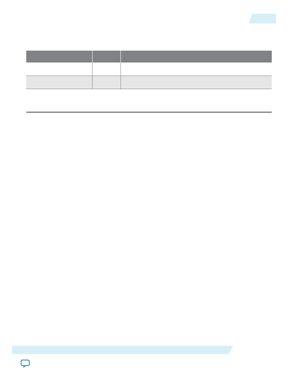
Table 4-14: 1-Bit Interface Signals
Signal
Direction
Description
tx_out[7:0]
(1)
Output
Transmit output. These signals are the serial outputs of lanes 7–0.
rx_in[7:0]
(1)
Input
Receive input. These signals are the serial inputs of lanes 7–0.
Note:
1. The x1 IP core only has lane 0. The x2 IP core only has lanes 1–0. The x4 IP core only has lanes 3–0.
Refer to Pin-out Files for Altera Devices for pin-out tables for all Altera devices in .pdf, .txt, and .xls
formats.
Transceiver channels are arranged in groups of six. For GX devices, the lowest six channels on the left side
of the device are labeled GXB_L0, the next group is GXB_L1, and so on. Channels on the right side of the
device are labeled GXB_R0, GXB_R1, and so on. Be sure to connect the Hard IP for PCI Express on the
left side of the device to appropriate channels on the left side of the device, as specified in the Pin-out Files
for Altera Devices.
Related Information
Physical Layout of Hard IP in Stratix V GX/GT/GS Devices
Stratix V devices include one, two, or four Hard IP for PCI Express IP cores. The following figures
illustrate the placement of the PCIe IP cores, transceiver banks, and channels for the largest Stratix V
devices. Note that the bottom left hard IP block includes the CvP functionality for flip chip packages. For
other package types, the CvP functionality is in the bottom right block. All other Hard IP blocks do not
include the CvP functionality.
UG-01097_avmm
2014.12.15
Serial Data Signals
4-27
64- or 128-Bit Avalon-MM Interface to the Application Layer
Altera Corporation