Altera Stratix V Avalon-MM Interface for PCIe Solutions User Manual
Page 43
Signal
Direction
Description
even if the V
VCCPGM
of the bank is not 3.3V if the following 2
conditions are met:
• The input signal meets the V
IH
and V
IL
specification for
LVTTL.
• The input signal meets the overshoot specification for 100°C
operation as specified by the “Maximum Allowed Overshoot
and Undershoot Voltage” section in volume 3 of the Stratix V
Device Handbook.
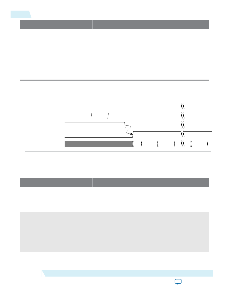
Figure 4-3: Reset and Link Training Timing Relationships
The following figure illustrates the timing relationship between
npor
and the LTSSM L0 state.
npor
IO_POF_Load
PCIe_LinkTraining_Enumeration
dl_ltssm[4:0]
detect detect.active polling.active
L0
Note: To meet the 100 ms system configuration time, you must use the fast passive parallel configuration
scheme with CvP and a 32-bit data width (FPP x32) or use the CvP in autonomous mode.
Table 4-6: Status and Link Training Signals
Signal
Direction
Description
cfg_par_err
Output
Indicates that a parity error in a TLP routed to the internal
Configuration Space. This error is also logged in the Vendor
Specific Extended Capability internal error register. You must
reset the Hard IP if this error occurs.
derr_cor_ext_rcv
Output
Indicates a corrected error in the RX buffer. This signal is for
debug only. It is not valid until the RX buffer is filled with data.
This is a pulse, not a level, signal. Internally, the pulse is
generated with the 500 MHz clock. A pulse extender extends the
signal so that the FPGA fabric running at 250 MHz can capture
it. Because the error was corrected by the IP core, no Application
Layer intervention is required.
(3)
4-10
Reset
UG-01097_avmm
2014.12.15
Altera Corporation
64- or 128-Bit Avalon-MM Interface to the Application Layer