2 adcl and adch – the adc data register, 3 didr0 – digital input disable register 0, Didr0 – Rainbow Electronics ATmega8HVD User Manual
Page 98: Atmega4hvd/8hvd
98
8052B–AVR–09/08
ATmega4HVD/8HVD
17.8.2
ADCL and ADCH – The ADC Data Register
When an ADC conversion is complete, the result is found in these two registers.When ADCL
is read, the ADC Data Register is not updated until ADCH is read.
• ADC9:0: ADC Conversion Result
These bits represent the result from the conversion, as detailed in
17.8.3
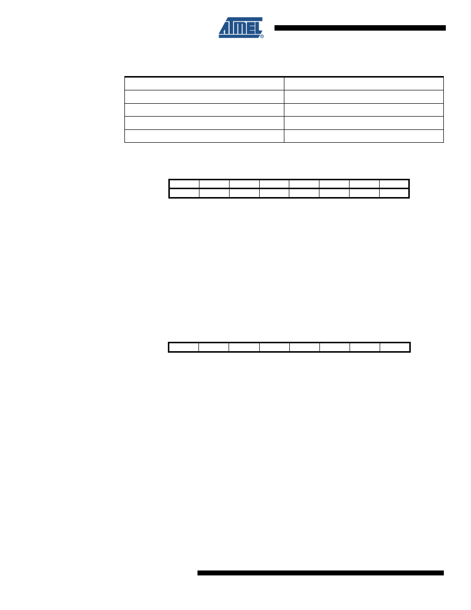
DIDR0 – Digital Input Disable Register 0
• Bit 7:1 – RES: Reserved
These bits are reserved for future use. To ensure compatibility with future devices, these bits
must always be written to zero when DIDR0 is written.
• Bit 0 – PB0DID: PB0 Digital Input Disable
When this bit is written logic one, the digital input buffer on the Port B pin is disabled. The PIN
register bit will always read as zero when this bit is set. When an analog signal is applied to
the PB0 pin and the digital input from this pin is not needed, this bit should be written logic one
to reduce power consumption in the digital input buffer.
Table 17-3.
ADC Channel Input Selection
ADMUX1:0
Input
00
VCELL
01
VTEMP
10
Reserved
11
ADC0
Bit
15
14
13
12
11
10
9
8
–
–
–
–
–
–
ADC9
ADC8
ADCH
ADC7
ADC6
ADC5
ADC4
ADC3
ADC2
ADC1
ADC0
ADCL
7
6
5
4
3
2
1
0
Read/Write
R
R
R
R
R
R
R
R
R
R
R
R
R
R
R
R
Initial Value
0
0
0
0
0
0
0
0
0
0
0
0
0
0
0
0
Bit
7
6
5
4
3
2
1
0
-
-
-
-
-
-
-
PB0DID
DIDR0
Read/Write
R
R
R
R
R
R
R
R/W
Initial Value
0
0
0
0
0
0
0
0