5 adc voltage reference, 6 adc noise canceler, Atmega4hvd/8hvd – Rainbow Electronics ATmega8HVD User Manual
Page 92: The reference voltage for the adc (v, Is taken from the internal 1.1v bandgap reference
92
8052B–AVR–09/08
ATmega4HVD/8HVD
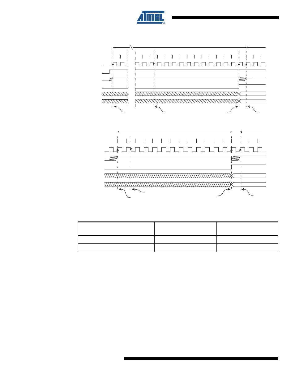
Figure 17-2. ADC Timing Diagram, First Conversion (Single Conversion Mode)
Figure 17-3. ADC Timing Diagram, Single Conversion
17.5
ADC Voltage Reference
The reference voltage for the ADC (V
REF
) is taken from the internal 1.1V bandgap reference.
17.6
ADC Noise Canceler
The ADC features a noise canceler that enables conversion during sleep mode to reduce
noise induced from the CPU core and other I/O peripherals. The noise canceler can be used
with Idle mode. To make use of this feature, the following procedure should be used:
1.
Make sure that the ADC is enabled and is not busy converting and the ADC conversion
complete interrupt is enabled.
2.
Enter ADC Noise Reduction mode. The ADC will start a conversion once the CPU has
been halted.
3.
If no other interrupts occur before the ADC conversion completes, the ADC interrupt
will wake up the CPU and execute the ADC Conversion Complete interrupt routine. If
Table 17-1.
ADC Conversion Time, except VTEMP input.
Condition
Sample & Hold (Cycles
from Start of Conversion)
Conversion Time (Cycles)
First conversion
15.5
27
Normal conversions
1.5
13
Sign and MSB of Result
LSB of Result
ADC Clock
ADSC
Sample & Hold
ADIF
ADCH
ADCL
Cycle Number
ADEN
1
2
26
27
14
15
16
17
18
19
20
21
22
23
24
25
1
2
First Conversion
Next
Conversion
3
MUX
Update
MUX
Update
Conversion
Complete
1
2
3
4
5
6
7
8
9
10
11
12
13
Sign and MSB of Result
LSB of Result
ADC Clock
ADSC
ADIF
ADCH
ADCL
Cycle Number
1
2
One Conversion
Next Conversion
3
Sample & Hold
MUX
Update
Conversion
Complete
MUX
Update