1 high voltage ports as general digital outputs, 1 configuring the pin, 2 reading the pin – Rainbow Electronics ATmega8HVD User Manual
Page 57: 2 alternate port functions, High voltage ports as general, Atmega4hvd/8hvd
57
8052B–AVR–09/08
ATmega4HVD/8HVD
13.1
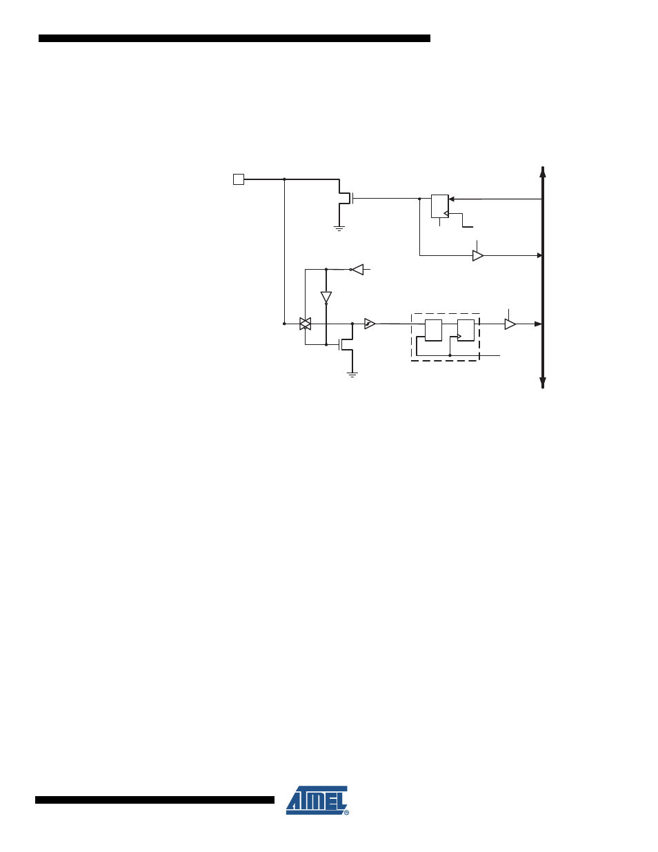
High Voltage Ports as General Digital Outputs
The high voltage ports are high voltage tolerant open collector output ports.
Figure 13-2
shows
a functional description of one output port pin, here generically called Pxn.
Figure 13-2. General High Voltage Digital I/O
(1)
Note:
1. WRx, RRx and RPx are common to all pins within the same port. clk
I/O
and SLEEP are com-
mon to all ports.
13.1.1
Configuring the Pin
Each port pin consist of two register bits: PORTxn and PINxn. As shown in
, the PORTxn bits are accesed at the PORTx I/O address, and the PINxn bits
at the PINx I/O address.
If PORTxn is written logic one, the port pin is driven low (zero). If PORTxn is written logic zero,
the port pin is tri-stated. The port pins are tri-stated when a reset condition becomes active,
even if no clocks are running.
13.1.2
Reading the Pin
The port pin can be read throughthe PINxn Register bit. As shown in
Figure 13-2
, the PINxn
Register bit and the preceding latch constitute a synchronizer. This is needed to avoid meta-
stability if the physical pin changes value near the edge of the internal clock, but it also
introduces a delay.
13.2
Alternate Port Functions
The High Voltage I/O has an alternate port function in addition to being general digital I/O.
Fig-
ure 13-3
shows how the port pin control signals from the simplified
Figure 13-2
can be
overridden by alternate functions.
WRx
SLEEP:
SLEEP CONTROL
clkI/O:
I/O CLOCK
SLEEP
Pxn
Q D
Q
PORTxn
_
CLR
D
ATA
B
U
S
RRx
SYNCHRONIZER
Q
D
CLR
PINxn
clk
I/O
Q
_
D
L
Q
Q
SET
CLR
_
RESET
RPx
RRx:
READ PORTx REGISTER
WRx:
WRITE PORTx REGISTER
RPx:
READ PINx REGISTER