1 alternate functions of port b, Atmega4hvd/8hvd – Rainbow Electronics ATmega8HVD User Manual
Page 69
69
8052B–AVR–09/08
ATmega4HVD/8HVD
14.3.1
Alternate Functions of Port B
The Port B pins with alternate functions are shown in
.
The alternate pin configuration is as follows:
• MISO/CKOUT/T1 - Port B, Bit 2
MISO : Slave Data Output pin for SPI programming
When not operating in programming mode, this pin can serve as Clock Output, CPU clock
divided by 2. When not operating in programming mode or as clock output, the pin can be
used as clock input for Time/Counter1
• SCK/SGND/T0 - Port B, Bit 1
SCK : Clock Input pin for SPI programming
When not operating in programming mode, this pin can serve as ground reference for ADC0
channel by configuring the pin as output low. When not used as SGND, the pin can be used as
clock input for Time/Counter0.
• ADC0 - Port B, Bit 0
Analog to Digital Converter, channel 0.
.
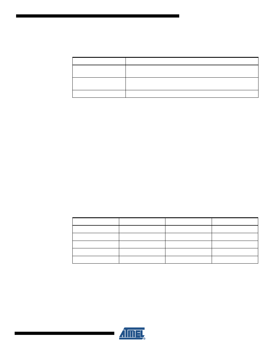
Table 14-3.
Port B Pins Alternate Functions
Port Pin
Alternate Function
PB2
MISO/CKOUT/T1 (SPI Bus Serial DataOutput, Clock Output,
Timer/Counter Clock Input)
PB1
SCK/SGND/T0 (SPI Bus Master Clock input, GND for ADC0
measurements, Timer/Counter 0 Clock Input)
PB0
ADC0 (ADC Input Channel 0)
Table 14-4.
Overriding Signals for Alternate Functions in PB2:0
Signal Name
PB2/MISO/CKOUT/T1
PB1/SCK/SGND/T0
PB0/ADC0