1 eeprom write prevents writing to spmcsr, 2 setting the lock bits from software, 3 reading the fuse and lock bits from software – Rainbow Electronics ATmega8HVD User Manual
Page 123: 4 preventing flash corruption, Atmega4hvd/8hvd
123
8052B–AVR–09/08
ATmega4HVD/8HVD
23.5.1
EEPROM Write Prevents Writing to SPMCSR
Note that an EEPROM write operation will block all software programming to Flash. Reading
the Fuses and Lock bits from software will also be prevented during the EEPROM write opera-
tion. It is recommended that the user checks the status bit (EEWE) in the EECR Register and
verifies that the bit is cleared before writing to the SPMCSR Register.
23.5.2
Setting the Lock Bits from Software
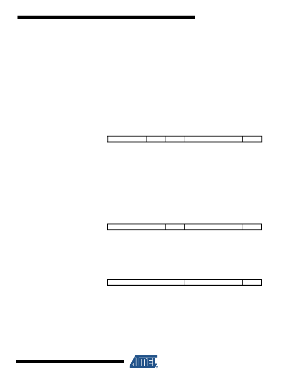
To set the Lock Bits, write the desired data to R0. If bits 1..0 in R0 are cleared (zero), the cor-
responding Lock bit will be programmed if an SPM instruction is executed within four cycles
after RFLB and SPMEN are set in SPMCSR. The Z-pointer is don’t care during this operation,
but for future compatibility it is recommended to load the Z-pointer with 0x0001 (same as used
for reading the lOck bits). For future compatibility it is also recommended to set bit 7..2 in R0 to
“1” when writing the Lock bits. When programming the Lock bits the entire Flash can be read
during the operation.
See
Table 24-1 on page 129
and
Table 24-2 on page 129
for how the different settings of the
Lock bits affect the Flash access.
23.5.3
Reading the Fuse and Lock Bits from Software
It is possible to read both the Fuse and Lock bits from software. To read the Lock bits, load the
Z-pointer with 0x0001 and set the RFLB and SPMEN bits in SPMCSR. When an LPM instruc-
tion is executed within three CPU cycles after the RFLB and SPMEN bits are set in SPMCSR,
the value of the Lock bits will be loaded in the destination register. The RFLB and SPMEN bits
will auto-clear upon completion of reading the Lock bits or if no LPM instruction is executed
within three CPU cycles or no SPM instruction is executed within four CPU cycles. When
RFLB and SPMEN are cleared, LPM will work as described in the Instruction set Manual.
The algorithm for reading the Fuse Low byte is similar to the one described above for reading
the Lock bits. To read the Fuse Low byte, load the Z-pointer with 0x0000 and set the RFLB
and SPMEN bits in SPMCSR. When an LPM instruction is executed within three cycles after
the RFLB and SPMEN bits are set in the SPMCSR, the value of the Fuse Low byte (FLB) will
be loaded in the destination register as shown below. Refer to
Table 24-4 on page 130
for a
detailed description and mapping of the Fuse Low byte.
Fuse and Lock bits that are programmed, will be read as zero. Fuse and Lock bits that are
unprogrammed, will be read as one.
23.5.4
Preventing Flash Corruption
During periods of low V
CC
, the Flash program can be corrupted because the supply voltage is
too low for the CPU and the Flash to operate properly. These issues are the same as for board
level systems using the Flash, and the same design solutions should be applied.
A Flash program corruption can be caused by two situations when the voltage is too low. First,
a regular write sequence to the Flash requires a minimum voltage to operate correctly. Sec-
Bit
7
6
5
4
3
2
1
0
R0
1
1
1
1
1
1
LB2
LB1
Bit
7
6
5
4
3
2
1
0
Rd
–
–
–
–
–
–
LB2
LB1
Bit
7
6
5
4
3
2
1
0
Rd
FLB7
FLB6
FLB5
FLB4
FLB3
FLB2
FLB1
FLB0