2 serial programming instruction set, Atmega4hvd/8hvd – Rainbow Electronics ATmega8HVD User Manual
Page 133
133
8052B–AVR–09/08
ATmega4HVD/8HVD
address. When using EEPROM page access only byte locations loaded with the Load
EEPROM Memory Page instruction is altered. The remaining locations remain
unchanged. If polling (RDY/BSY) is not used, the used must wait at least t
WD_EEPROM
before issuing the next page (See
Table 24-9
). In a chip erased device, no 0xFF in the
data file(s) need to be programmed.
6.
Any memory location can be verified by using the Read instruction which returns the
content at the selected address at serial output MISO.
7.
At the end of the programming session, RESET can be set high to commence normal
operation.
8.
Power-off sequence (if needed):
Set RESET to “1”.
Turn V
CC
power off.
24.6.2
Serial Programming Instruction set
Table 24-10 on page 133
and
Figure 24-2 on page 135
describes the Instruction set.
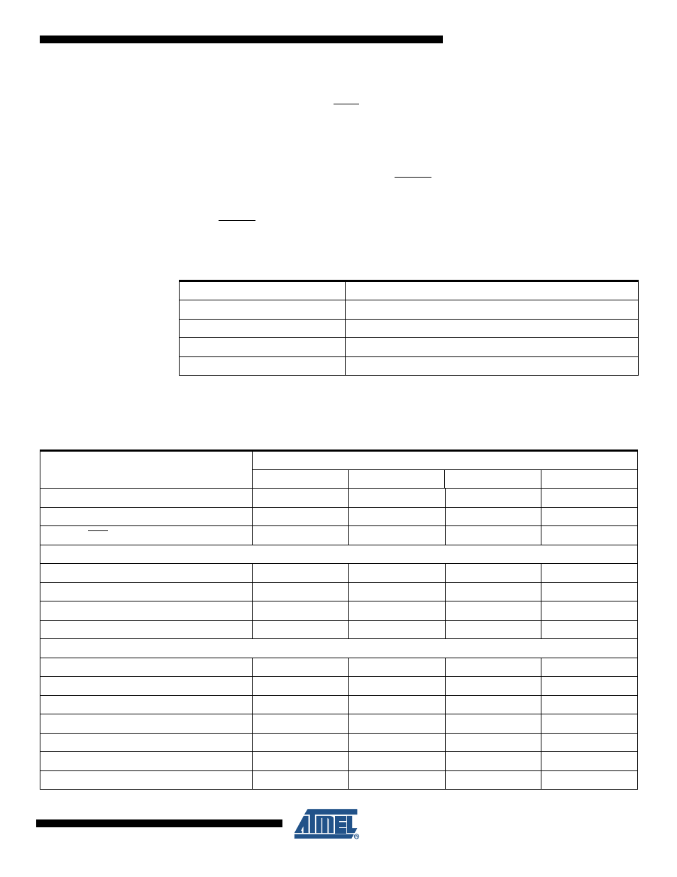
Table 24-9.
Minimum Wait Delay Before Writing the Next Flash or EEPROM Location
Symbol
Minimum Wait Delay
t
WD_FLASH
4.5 ms
t
WD_EEPROM
4.0 ms
t
WD_ERASE
4.0 ms
t
WD_FUSE
4.5 ms
Table 24-10. Serial Programming Instruction Set
Instruction/Operation
Instruction Format
Byte 1
Byte 2
Byte 3
Byte4
Programming Enable
$AC
$53
$00
$00
Chip Erase (Program Memory/EEPROM)
$AC
$80
$00
$00
Poll RDY/BSY
$F0
$00
$00
data byte out
Load Instructions
Load Extended Address byte
$4D
$00
Extended adr
$00
Load Program Memory Page, High byte
$48
adr MSB
adr LSB
high data byte in
Load Program Memory Page, Low byte
$40
adr MSB
adr LSB
low data byte in
Load EEPROM Memory Page (page access)
$C1
$00
adr LSB
data byte in
Read Instructions
Read Program Memory, High byte
$28
adr MSB
adr LSB
high data byte out
Read Program Memory, Low byte
$20
adr MSB
adr LSB
low data byte out
Read EEPROM Memory
$A0
adr MSB
adr LSB
data byte out
Read Lock bits
$58
$00
$00
data byte out
Read Signature Byte
$30
$00
adr LSB
data byte out
Read Fuse bits
$50
$00
$00
data byte out
Read Fuse High bits
$58
$08
$00
data byte out