1 compare match blocking by tcnt0 write, 2 using the output compare unit, 8 timer/counter timing diagrams – Rainbow Electronics ATmega8HVD User Manual
Page 81: Atmega4hvd/8hvd
81
8052B–AVR–09/08
ATmega4HVD/8HVD
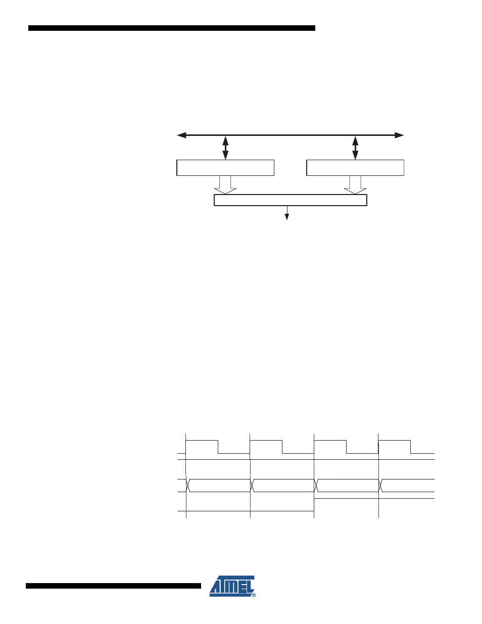
OCFnA as there is only one Output Compare Unit. If the corresponding interrupt is enabled,
the Output Compare Flag generates an Output Compare interrupt. The Output Compare Flag
is automatically cleared when the interrupt is executed. Alternatively, the flag can be cleared
by software by writing a logical one to its I/O bit location.
Figure 16-5 on page 81
shows a
block diagram of the Output Compare unit.
Figure 16-5. Output Compare Unit, Block Diagram
16.7.1
Compare Match Blocking by TCNT0 Write
All CPU write operations to the TCNTnH/L Register will block any Compare Match that occur
in the next timer clock cycle, even when the timer is stopped. This feature allows OCRnA/B to
be initialized to the same value as TCNTn without triggering an interrupt when the
Timer/Counter clock is enabled.
16.7.2
Using the Output Compare Unit
Since writing TCNTnH/L will block all Compare Matches for one timer clock cycle, there are
risks involved when changing TCNTnH/L when using the Output Compare Unit, independently
of whether the Timer/Counter is running or not. If the value written to TCNTnH/L equals the
OCRnA/B value, the Compare Match will be missed.
16.8
Timer/Counter Timing Diagrams
The Timer/Counter is a synchronous design and the timer clock (clk
Tn
) is therefore shown as a
clock enable signal in the following figures. The figures include information on when Interrupt
Flags are set.
Figure 16-6 on page 81
contains timing data for basic Timer/Counter operation.
The figure shows the count sequence close to the MAX value.
Figure 16-6. Timer/Counter Timing Diagram, no Prescaling
Figure 16-7 on page 82
shows the same timing data, but with the prescaler enabled.
OCFn
x (Int.Req.)
=
(8/16-bit Comparator )
OCRnx
DATA BUS
TCNTn
clk
Tn
(clk
I/O
/1)
TOVn
clk
I/O
TCNTn
MAX - 1
MAX
BOTTOM
BOTTOM + 1