1 alternate functions of port c, Atmega4hvd/8hvd – Rainbow Electronics ATmega8HVD User Manual
Page 59
59
8052B–AVR–09/08
ATmega4HVD/8HVD
13.2.1
Alternate Functions of Port C
The Port C pins with alternate functions are shown in
Table 13-2
.
The alternate pin configuration is as follows:
• INT0/ICP0/XTAL - Port C, Bit 0
INT0, External Interrupt 0: When INT0 is written to one and the I-bit in the Status Register
(SREG) is set (one), the corresponding external pin interrupt is enabled. The Interrupt Sense
Control bits in the
”EICRA – External Interrupt Control Register A” on page 53
- defines
whether the external interrupt is activated on rising or falling edge or level sensed. Activity on
any of these pins will trigger an interrupt request even if the pin is enabled as an output. This
provides a way of generating a software interrupt.
XTAL, External Clock: When the CKSEL fuse is programmed, PC0 is used as clock source
instead of the Internal RC oscillator (For test purposes only).
• MOSI/INT1/EXT_PROT - Port C, Bit 1
MOSI, Slave Data Input pin for SPI Programming.
INT1, External Interrupt 1: When INT1 is written to one and the I-bit in the Status Register
(SREG) is set (one), the corresponding external pin interrupt is enabled. The Interrupt Sense
Control bits in the
”EICRA – External Interrupt Control Register A” on page 53
- defines
whether the external interrupt is activated on rising or falling edge or level sensed. Activity on
any of these pins will trigger an interrupt request even if the pin is enabled as an output. This
provides a way of generating a software interrupt.
EXT_PROT, External Protection Input: When the EPID bit in the BPCR Register is cleared,
the External Protection Input functionality is enabled. Note that this port overriding is default
enabled.
Table 13-3
relates the alternate functions of Port C to the overriding signals shown in
Figure
13-3 on page 58
.
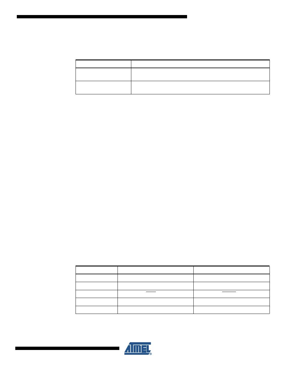
Table 13-2.
Port C Pins Alternate Functions
Port Pin
Alternate Function
PC0
INT0/ICP0/XTAL (External Interrupt 0, Timer/Counter 0 input Capture
Trigger or External Clock)
PC1
MOSI/INT1/EXT_PROT (SPI BUS Serial Data Input, External Interrupt
1, External Protection Input)
Table 13-3.
Overriding Signals for Alternate Functions in PC1:0
Signal Name
PC1/MOSI/INT1/EXT_PROT
PC0/INT0/ICP0/XTAL
PVOE
0
0
PVOV
0
0
DIEOE
INT Enable + EPID
INT Enable + CKSEL
DIEOV
1
1
DI
INT1/EXT_PROT
INT0/ICP0/XTAL INPUT