Atmega4hvd/8hvd, Figure 13-3. high voltage digital i/o – Rainbow Electronics ATmega8HVD User Manual
Page 58
58
8052B–AVR–09/08
ATmega4HVD/8HVD
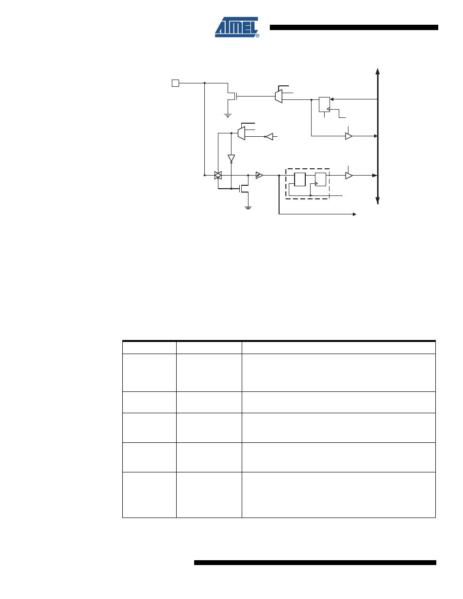
Figure 13-3. High Voltage Digital I/O
(1)
Note:
1. WRx, RRx and RPx are common to all pins within the same port. clk
I/O
and SLEEP are com-
mon to all ports. All other signals are unique for each pin.
Table 13-1
summarizes the function of the overriding signals. The pin and port indexes from
Figure 13-3
are not shown in the succeeding tables. The overriding signals are generated
internally in the modules having the alternate function.
Table 13-1.
Generic Description of Overriding Signals for Alternate Functions
Signal Name
Full Name
Description
PVOE
Port Value
Override Enable
If this signal is set and the Output Driver is enabled, the port
value is controlled by the PVOV signal. If PVOE is cleared,
and the Output Driver is enabled, the port Value is controlled
by the PORTxn Register bit.
PVOV
Port Value
Override Value
If PVOE is set, the port value is set to PVOV, regardless of the
setting of the PORTxn Register bit.
DIEOE
Digital Input
Enable Override
Enable
If this bit is set, the Digital Input Enable is controlled by the
DIEOV signal. If this signal is cleared, the Digital Input Enable
is determined by MCU state (Normal mode, sleep mode).
DIEOV
Digital Input
Enable Override
Value
If DIEOE is set, the Digital Input is enabled/disabled when
DIEOV is set/cleared, regardless of the MCU state (Normal
mode, sleep mode).
DI
Digital Input
This is the Digital Input to alternate functions. In the figure, the
signal is connected to the output of the schmitt trigger but
before the synchronizer. Unless the Digital Input is used as a
clock source, the module with the alternate function will use
its own synchronizer.
WRx
PVOVxn
PVOExn
PVOExn:
Pxn PORT VALUE OVERRIDE ENABLE
PVOVxn:
Pxn PORT VALUE OVERRIDE VALUE
DIEOExn: Pxn DIGITAL INPUT-ENABLE OVERRIDE ENABLE
DIEOVxn: Pxn DIGITAL INPUT-ENABLE OVERRIDE VALUE
SLEEP
Pxn
DIEOExn
DIEOVxn
Q D
Q
PORTxn
_
CLR
1
0
1
0
DA
T
A
B
U
S
RRx
SYNCHRONIZER
Q
D
CLR
PINxn
clk
I/O
Q
_
D
L
Q
Q
SET
CLR
_
RESET
RPx
DIxn
RRx:
READ PORTx REGISTER
WRx:
WRITE PORTx REGISTER
RPx:
READ PINx REGISTER
clk
I/O
:
I/O CLOCK
DIxn:
DIGITAL INPUT PIN n ON PORTx
SLEEP:
SLEEP CONTROL