7 high-voltage serial programming, Atmega4hvd/8hvd – Rainbow Electronics ATmega8HVD User Manual
Page 135
135
8052B–AVR–09/08
ATmega4HVD/8HVD
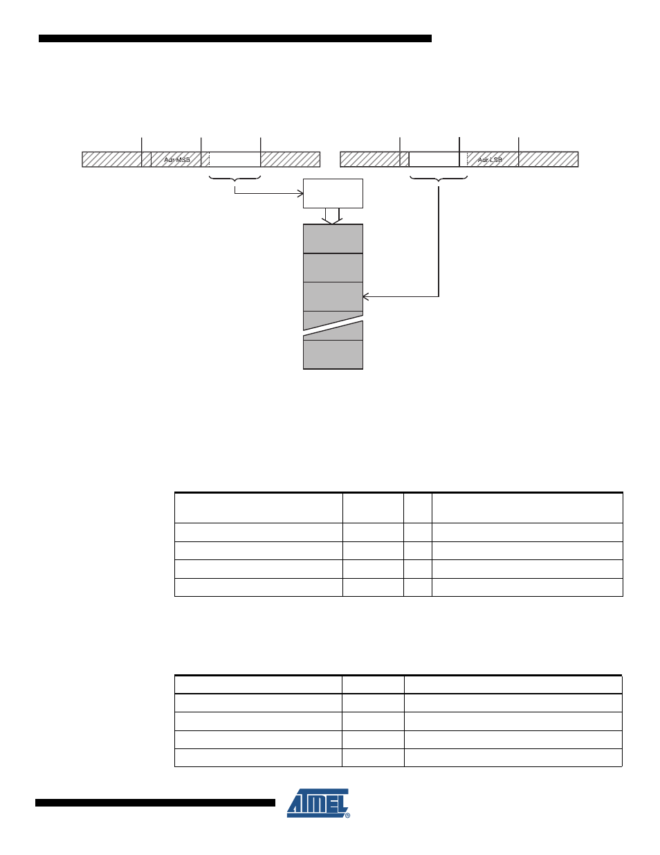
Figure 24-2. Serial Programming Instruction example
24.7
High-voltage Serial Programming
This section describes how to program and verify Flash Program memory, EEPROM Data
memory, Lock bits and Fuse bits in the ATmega4HVD/8HVD.
The prog_enable minimum period for the Serial Clock Input (SCI) during High-voltage Serial
Programming is 220 ns.
Byte 1
Byte 2
Byte 3
Byte 4
Adr LSB
Bit 15 B
0
Serial Programming Instruction
Program Memory/
EEPROM Memory
Page 0
Page 1
Page 2
Page N-1
Page Buffer
Write Program Memory Page/
Write EEPROM Memory Page
Load Program Memory Page (High/Low Byte)/
Load EEPROM Memory Page (page access)
Byte 1
Byte 2
Byte 3
Byte 4
Bit 15 B
0
Adr MSB
Page Offset
Page Number
Adr M
MS
SB
A
A
Adrr L
LSB
B
Table 24-11. Pin Name Mapping
Signal Name in High-voltage
Serial Programming Mode
Pin Name
I/O
Function
SDO
PB1
O
Serial Data Output
SDI
PC1
I
Serial Data Input
SII
PB0
I
Serial Instruction Input
SCI
PC0
I
Serial Clock Input (min. 220ns period)
Table 24-12. Pin Values Used to Enter Programming Mode
Symbol
Pin Name
Value
Prog_enable[0]
PB0
0
Prog_enable[1]
PB1
0
Prog_enable[2]
NC
0
Prog_enable[3]
PB2
0