3 chip erase, 4 programming the flash, Atmega4hvd/8hvd – Rainbow Electronics ATmega8HVD User Manual
Page 137
137
8052B–AVR–09/08
ATmega4HVD/8HVD
24.8.3
Chip Erase
The Chip Erase will erase the Flash and EEPROM
(1)
memories plus Lock bits. The Lock bits
are not reset until the Program memory has been completely erased. The Fuse bits are not
changed. A Chip Erase must be performed before the Flash and/or EEPROM are re-
programmed.
Note:
1. The EEPROM memory is preserved during Chip Erase if the EESAVE Fuse is programmed.
1.
Load command “Chip Erase” (see
Table 24-14
).
2.
Wait after Instr. 3 until SDO goes high for the “Chip Erase” cycle to finish.
3.
Load Command “No Operation”.
24.8.4
Programming the Flash
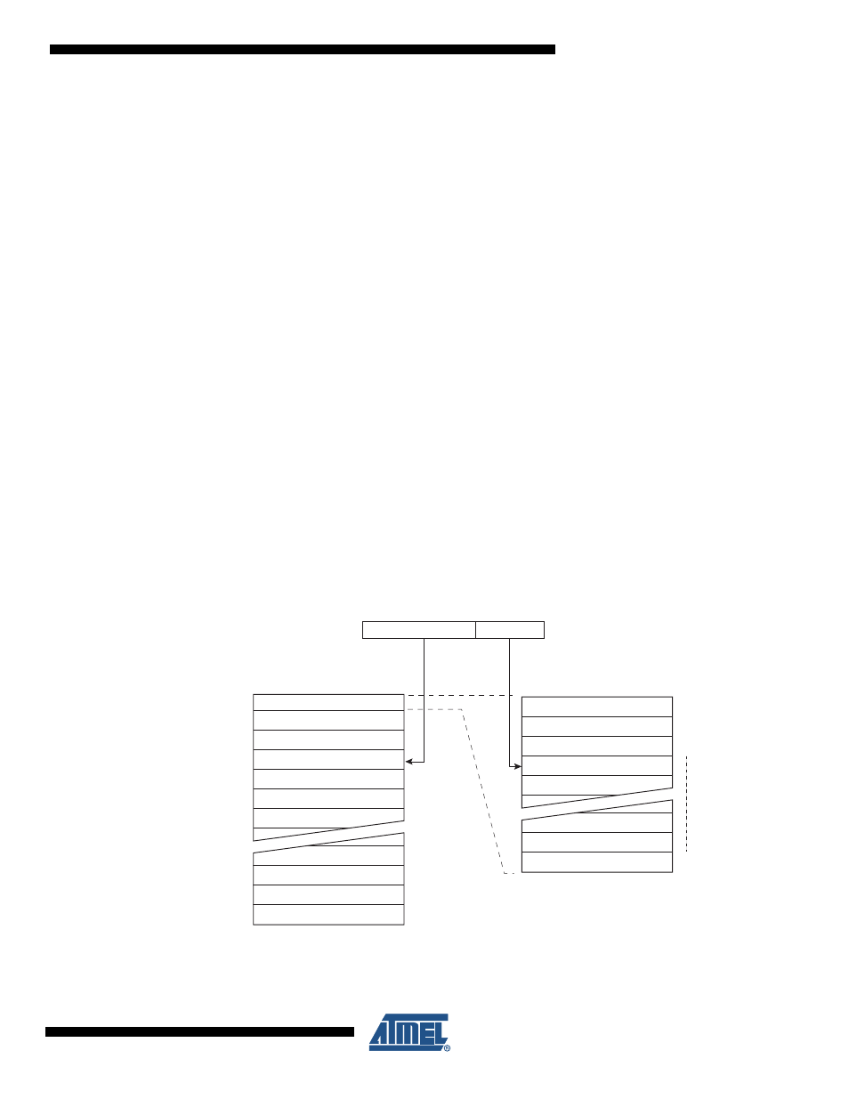
The Flash is organized in pages, see
Table 24-10 on page 133
. When programming the Flash,
the program data is latched into a page buffer. This allows one page of program data to be
programmed simultaneously. The following procedure describes how to program the entire
Flash memory:
1.
Load Command “Write Flash” (see
Table 24-14
).
2.
Load Flash Page Buffer.
3.
Load Flash High Address and Program Page. Wait after Instr. 3 until SDO goes high
for the “Page Programming” cycle to finish.
4.
Repeat 2 through 3 until the entire Flash is programmed or until all data has been
programmed.
5.
End Page Programming by Loading Command “No Operation”.
When writing or reading serial data to the ATmega4HVD/8HVD, data is clocked on the rising
edge of the serial clock, see
Figure 24-4
,
Figure 26-3
and
Table 26-9
for details.
Figure 24-3. Addressing the Flash which is Organized in Pages
PROGRAM MEMORY
WORD ADDRESS
WITHIN A PAGE
PAGE ADDRESS
WITHIN THE FLASH
INSTRUCTION WORD
PAGE
PCWORD[PAGEMSB:0]:
00
01
02
PAGEEND
PAGE
PCWORD
PCPAGE
PCMSB
PAGEMSB
PROGRAM
COUNTER