4 eeprom data memory, 1 eeprom read/write access, 5 i/o memory – Rainbow Electronics ATmega8HVD User Manual
Page 16: Atmega4hvd/8hvd
16
8052B–AVR–09/08
ATmega4HVD/8HVD
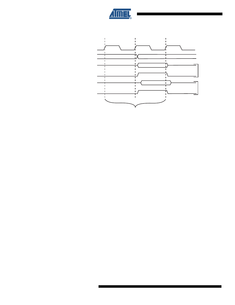
Figure 1. On-chip Data SRAM Access Cycles
7.4
EEPROM Data Memory
The ATmega4HVD/8HVD contains 256 bytes of data EEPROM memory. It is organized as a
separate data space, in which single bytes can be read and written. The EEPROM has an
endurance of at least 100,000 write/erase cycles. The access between the EEPROM and the
CPU is described in the following, specifying the EEPROM Address Registers, the EEPROM
Data Register, and the EEPROM Control Register.
For a detailed description of Serial and Parallel data downloading to the EEPROM, see
respectively.
7.4.1
EEPROM Read/Write Access
The EEPROM Access Registers are accessible in the I/O space.
The write access time for the EEPROM is given in
Table 7-1
. A self-timing function, however,
lets the user software detect when the next byte can be written. If the user code contains
instructions that write the EEPROM, some precautions must be taken.
In order to prevent unintentional EEPROM writes, a specific write procedure must be followed.
Refer to the description of the EEPROM Control Register for details on this.
When the EEPROM is read, the CPU is halted for four clock cycles before the next instruction
is executed. When the EEPROM is written, the CPU is halted for two clock cycles before the
next instruction is executed.
7.5
I/O Memory
The I/O space definition of the ATmega4HVD/8HVD is shown in
All ATmega4HVD/8HVD I/Os and peripherals are placed in the I/O space. All I/O locations
may be accessed by the LD/LDS/LDD and ST/STS/STD instructions, transferring data
between the 32 general purpose working registers and the I/O space. I/O Registers within the
address range 0x00 - 0x1F are directly bit-accessible using the SBI and CBI instructions. In
these registers, the value of single bits can be checked by using the SBIS and SBIC instruc-
clk
WR
RD
Data
Data
Address
Address valid
T1
T2
T3
Compute Address
Read
Wr
ite
CPU
Memory Access Instruction
Next Instruction