1 analog input circuitry, 2 analog noise canceling techniques, Atmega4hvd/8hvd – Rainbow Electronics ATmega8HVD User Manual
Page 93
93
8052B–AVR–09/08
ATmega4HVD/8HVD
another interrupt wakes up the CPU before the ADC conversion is complete, that inter-
rupt will be executed, and an ADC Conversion Complete interrupt request will be
generated when the ADC conversion completes. The CPU will remain in active mode
until a new sleep command is executed.
Note that the ADC will not be automatically turned off when entering sleep modes other than
Idle mode. The user is advised to write zero to ADEN before entering such sleep modes to
avoid excessive power consumption.
17.6.1
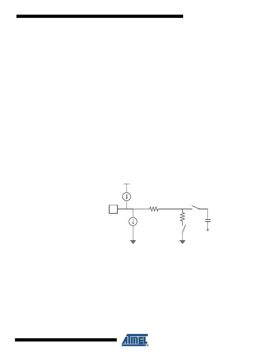
Analog Input Circuitry
The analog input circuitry is illustrated in
Figure 17-4
An analog source applied to ADCn is
subjected to the pin capacitance and input leakage of that pin, regardless of whether that
channel is selected as input for the ADC. When the channel is selected, the source must drive
the S/H capacitor through the series resistance (combined resistance in the input path).
The ADC is optimized for analog signals with an output impedance of approximately 10 k
Ω
or
less. If such a source is used, the sampling time will be negligible. If a source with higher
impedance is used, the sampling time will depend on how long time the source needs to
charge the S/H capacitor, which can vary widely. The user is recommended to only use low
impedant sources with slowly varying signals, since this minimizes the required charge trans-
fer to the S/H capacitor.
Signal components higher than the Nyquist frequency (f
ADC
/2) should not be present to avoid
distortion from unpredictable signal convolution. The user is advised to remove high frequency
components with a low-pass filter before applying the signals as inputs to the ADC.
Figure 17-4. Analog Input Circuitry
17.6.2
Analog Noise Canceling Techniques
Digital circuitry inside and outside the device generates EMI which might affect the accuracy of
analog measurements. If conversion accuracy is critical, the noise level can be reduced by
applying the following techniques:
1.
Keep analog signal paths as short as possible. Make sure analog tracks run over the
analog ground plane, and keep them well away from high-speed switching digital
tracks.
2.
Use the ADC noise canceler function to reduce induced noise from the CPU.
3.
If any port pins are used as digital outputs, it is essential that these do not switch while
a conversion is in progress.
ADCn
I
IH
TBD k
W
C
S/H
= TBD pF
V
CC
/2
I
IL
TBD k
W