Atmega4hvd/8hvd, Figure 14-5. alternate port functions, Data b u s – Rainbow Electronics ATmega8HVD User Manual
Page 67
67
8052B–AVR–09/08
ATmega4HVD/8HVD
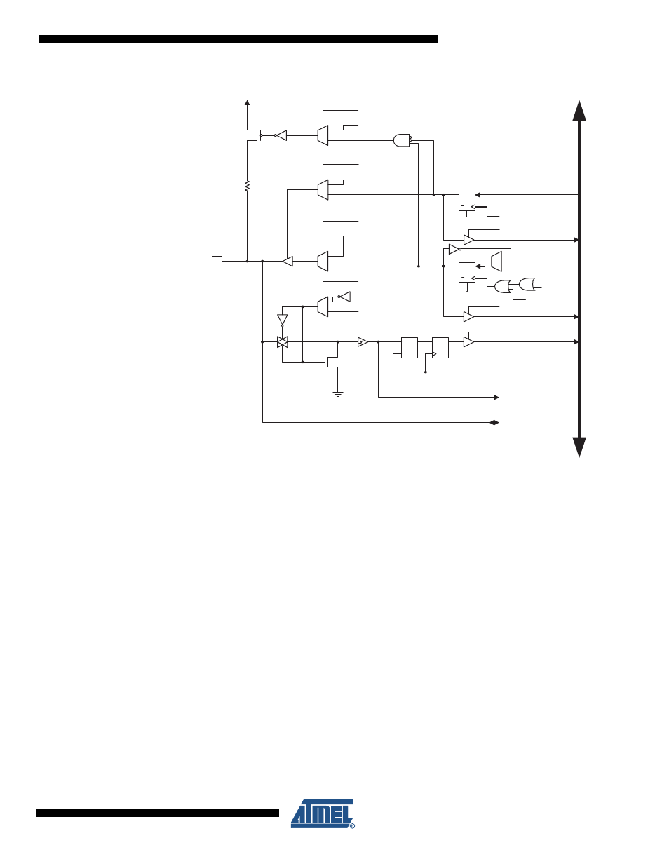
Figure 14-5. Alternate Port Functions
(1)
Note:
1. WRx, WPx, WDx, RRx, RPx, and RDx are common to all pins within the same port. clk
I/O
,
SLEEP, and PUD are common to all ports. All other signals are unique for each pin.
Table 14-2 on page 68
summarizes the function of the overriding signals. The pin and port
indexes from
Figure 14-5
are not shown in the succeeding tables. The overriding signals are
generated internally in the modules having the alternate function.
clk
RPx
RRx
WRx
RDx
WDx
PUD
SYNCHRONIZER
WDx:
WRITE DDRx
WRx:
WRITE PORTx
RRx:
READ PORTx REGISTER
RPx:
READ PORTx PIN
PUD:
PULLUP DISABLE
clk
I/O
:
I/O CLOCK
RDx:
READ DDRx
D
L
Q
Q
SET
CLR
0
1
0
1
0
1
DIxn
AIOxn
DIEOExn
PVOVxn
PVOExn
DDOVxn
DDOExn
PUOExn
PUOVxn
PUOExn:
Pxn PULL-UP OVERRIDE ENABLE
PUOVxn:
Pxn PULL-UP OVERRIDE VALUE
DDOExn:
Pxn DATA DIRECTION OVERRIDE ENABLE
DDOVxn:
Pxn DATA DIRECTION OVERRIDE VALUE
PVOExn:
Pxn PORT VALUE OVERRIDE ENABLE
PVOVxn:
Pxn PORT VALUE OVERRIDE VALUE
DIxn:
DIGITAL INPUT PIN n ON PORTx
AIOxn:
ANALOG INPUT/OUTPUT PIN n ON PORTx
RESET
RESET
Q
Q
D
CLR
Q
Q
D
CLR
Q
Q
D
CLR
PINxn
PORTxn
DDxn
D
ATA
B
U
S
0
1
DIEOVxn
SLEEP
DIEOExn: Pxn DIGITAL INPUT-ENABLE OVERRIDE ENABLE
DIEOVxn: Pxn DIGITAL INPUT-ENABLE OVERRIDE VALUE
SLEEP:
SLEEP CONTROL
Pxn
I/O
0
1
PTOExn
WPx
PTOExn:
Pxn, PORT TOGGLE OVERRIDE ENABLE
WPx:
WRITE PINx