Rainbow Electronics DS26503 User Manual
Page 36
DS26503 T1/E1/J1 BITS Element
36 of 123
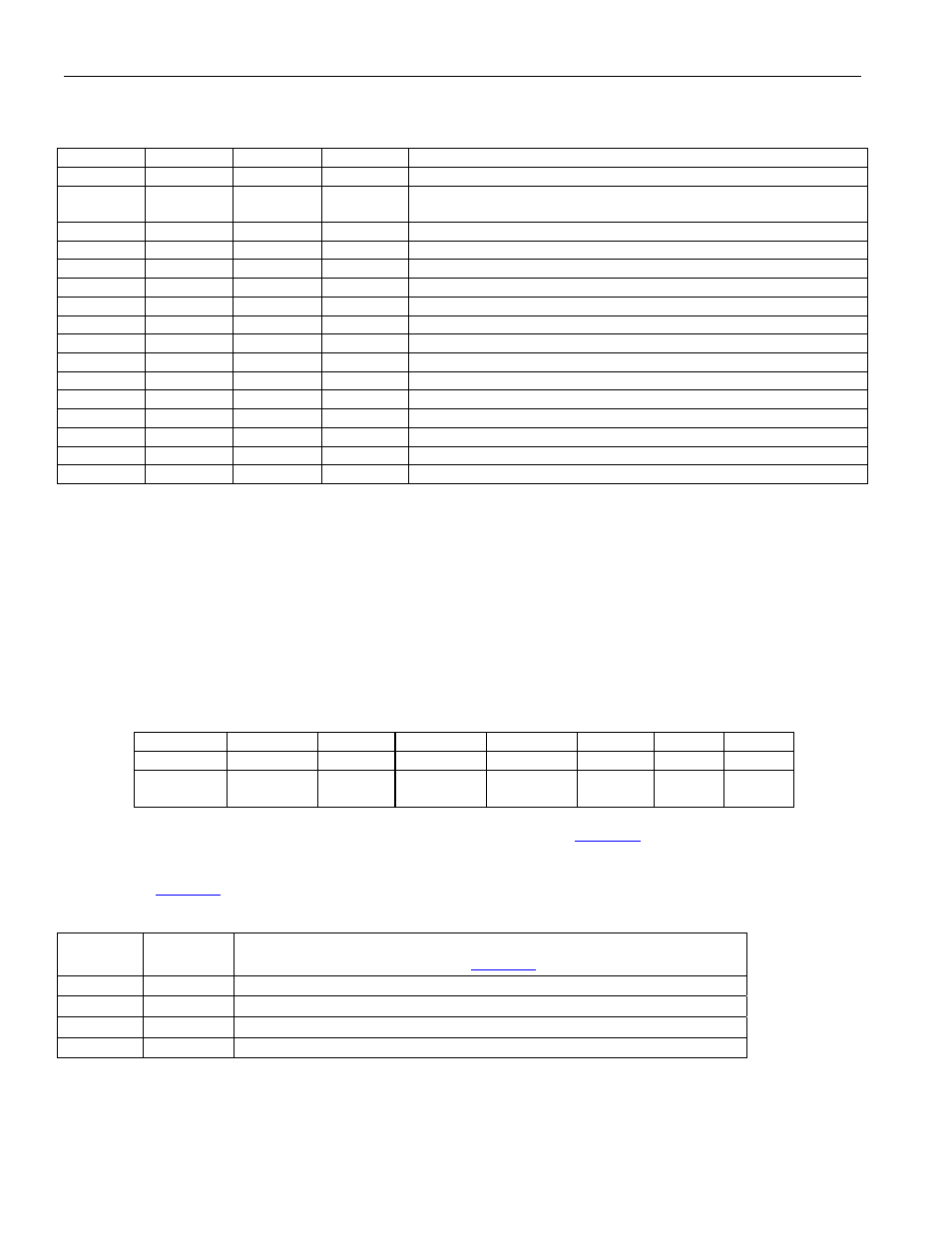
Bit 4-7/ Transmit Mode Configuration (TMODE[3:0]). Used to select the operating mode of the transmit path for the
DS26503.
TMODE3 TMODE2
TMODE1 TMODE0
Transmit Path Operating Mode
0
0
0
0
T1 D4
0 0 0 1
T1
ESF
(Note: In this mode the TFSE (T1TCR2.6) bit should be
set = 0.)
0
0
1
0
J1 D4
0
0
1
1
J1 ESF
0
1
0
0
E1 FAS
0
1
0
0
E1 FAS + CAS (Note 1)
0 1 0 1
Reserved
0 1 1 0
E1
CRC4
0
1
1
0
E1 CRC4 + CAS (Note 1)
0 1 1 1
Reserved
1
0
0
0
E1 G.703 2048 kHz Synchronization Interface
1 0 0 1
Reserved
1 0 1 0
Reserved
1
0
1
1
6312kHz Synchronization Interface (Note 2)
1 1 0 0
Reserved
1 1 0 1
Reserved
Note 1: The DS26503 does not have an internal source for CAS signaling and multiframe alignment generation. CAS signaling, and the
multiframe alignment word, must be embedded in the transmit data (in the TS16 position) present on the TSER pin and frame
aligned to sync signal on the TS pin.
Note 2: In addition to setting the TMODE bits to 6312kHz Synchronization Interface mode, the Transmit PLL must also be configured to
transmit a 6312kHz signal through the Transmit PLL Control Register (TPCR.6 and TPCR.7)
Register Name:
TPCR
Register Description:
Transmit PLL Control Register
Register Address:
09h
Bit
# 7 6 5 4 3 2
1
0
Name
TPLLOFS0 TPLLOFS1 PLLOS TPLLIFS0 TPLLIFS1 TPLLSS TCSS1 TCSS0
Default
0 0 0 0 0 0
0
0
HW
Mode
0 0 0 0 0 0
TCSS1
PIN 31
TCSS0
PIN 63
For more information on all the bits in the Transmit PLL control register, refer to
Bit 0-1/Transmit Clock (TX CLOCK) Source Select (TCSS[1:0]). These bits control the output of the TX PLL Clock Mux
function. See
TCSS1 TCSS0
Transmit Clock (TX CLOCK) Source
0
0
The TCLK pin is the source of transmit clock.
0
1
The PLL_CLK is the source of transmit clock.
1
0
The scaled signal present at MCLK as the transmit clock.
1
1
The signal present at RCLK is the transmit clock.
Bit 2/Transmit PLL_CLK Source Select (TPLLSS). Selects the reference signal for the TX PLL.
0 = Use the recovered network clock. This is the same clock available at the RCLK pin (output).
1 = Use the externally provided clock present at the TCLK pin.