Power-up sequence, Test reset register – Rainbow Electronics DS26503 User Manual
Page 34
DS26503 T1/E1/J1 BITS Element
34 of 123
7.3.1 Power-Up Sequence
The DS26503 contains an on-chip power-up reset function, which automatically clears the writeable
register space immediately after power is supplied to the device. The user can issue a chip reset at any
time. Issuing a reset will disrupt signals flowing through the DS26503 until the device is reprogrammed.
The reset can be issued through hardware using the TSTRST pin or through software using the SFTRST
function in the master mode register. The LIRST (LIC2.6) should be toggled from zero to one to reset the
line interface circuitry. (It will take the DS26503 about 40ms to recover from the LIRST bit being
toggled.)
7.3.2 Test Reset Register
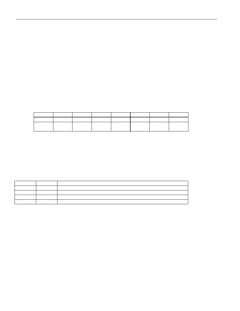
Register Name:
TSTRREG
Register Description:
Test Reset Register
Register Address:
00h
Bit
# 7 6 5 4 3 2 1 0
Name — —
TEST1
TEST0
— — —
SFTRST
Default
0 0 0 0 0 0 0 0
HW
Mode
X X X X X X X X
Bit 0/Software Issued Reset (SFTRST). A zero-to-one transition causes the register space in the DS26503 to be cleared. A
reset clears all configuration and status registers. The bit automatically clears itself when the reset has completed.
Bits 1-3/Unused, must be set = 0 for proper operation.
Bits 4-5/Test Mode Bits (TEST0, TEST1). Test modes are used to force the output pins of the DS26503 into known states.
This can facilitate the checkout of assemblies during the manufacturing process and also be used to isolate devices from shared
buses.
TEST1
TEST0
Effect On Output Pins
0 0
Operate
normally
0
1
Force all output pins into tri-state (including all I/O pins and parallel port pins)
1
0
Force all output pins low (including all I/O pins except parallel port pins)
1
1
Force all output pins high (including all I/O pins except parallel port pins)
Bits 6-7/Unused, must be set = 0 for proper operation.