2 sram interface, 1 sram slave writes, Sram interface 9.3.2.1 – Intel NETWORK PROCESSOR IXP2800 User Manual
Page 333: Sram slave writes, 121 example of target write to sram of 68 bytes

Hardware Reference Manual
333
Intel
®
IXP2800 Network Processor
PCI Unit
9.3.2
SRAM Interface
The SRAM interface connects the FBus to the internal push/pull command bus and the SRAM
push/pull data buses. Request to memory is sent on the command bus. Data request is received as
valid push/pull ID sent by the SRAM push/pull data bus.
If the PCI_SRAM_BAR is used, the target state machine generates a request to the command bus
for SRAM access. Once the grant is received, the address, then data is directed between the slave
FIFOs of the PCI core and the SRAM push/pull bus.
9.3.2.1
SRAM Slave Writes
The slave write buffer is used to support memory burst accesses. The buffer is added to guarantee
data transfer for each clock and burst size can be determined before memory request is issued. Data
is assembled in the buffers before being sent to memory for SRAM write.
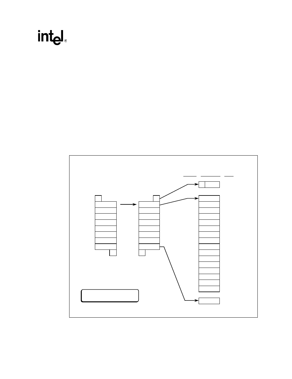
On the push/pull bus, AM access can start at any address and have length up to 16 Dwords as
shown in
. For masked writes, only size 1 is supported to transfer up to four bytes.
The slave interface also has to make sure there is enough data in the slave write buffer to complete
the memory data transfer before making a memory request.
Figure 121. Example of Target Write to SRAM of 68 Bytes
A9768-01
1111
0011
1111
1111
1111
1111
1111
1111
1111
1111
1111
00111111
00000000
00000000
00000000
00000000
00000000
00000000
00000000
00000000
11111100
1111
1111
1111
1111
1111
1111
1100
Memory Transfer
Internal
Bus Data
Byte Lane
PCI Bus
Byte Enables
Slave Write Burst to memory
Starting address = 0x4
Byte Enables
Address
Size
2 bytes
0x0
0x8
0x48
2 bytes
64 bytes
