2 pci pin protocol interface block, Pci pin protocol interface block, 119 data access paths – Intel NETWORK PROCESSOR IXP2800 User Manual
Page 321
Hardware Reference Manual
321
Intel
®
IXP2800 Network Processor
PCI Unit
9.2
PCI Pin Protocol Interface Block
This block generates the PCI compliant protocol logic. It operates either as an initiator or a target
device on the PCI Bus. As an initiator, all bus cycles are generated by the core. As a PCI target, the
core responds to bus cycles that have been directed towards it.
On the PCI Bus, the interface supports interrupts, 64-bit data path, 32-bit addressing, and single
configuration space. The local configuration registers are accessible from the PCI Bus or from the
Intel XScale
®
core through an internal path.
The PCI block interfaces with the other sub-blocks with a FIFO bus called FBus. The FBus speed
is the same as the internal Push/Pull bus speed. The FIFOs are implemented with clock
synchronization logic between the PCI speed and the internal Push/Pull bus speed.
There are four data FIFOs and two address FIFOs in the core. The separate slave and master data
FIFOs allows simultaneous operations and multiple outstanding PCI bus transfers.
lists
the FIFO sizes. The target address FIFO latches up to four PCI read or write addresses.
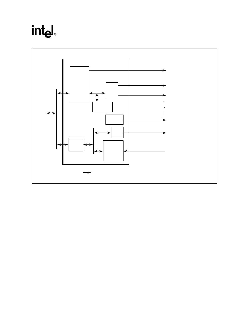
Figure 119. Data Access Paths
A9766-03
TGT CSR R/W
PCI UNIT
TGT DRAM R/W
TGT SRAM R/W
Local Internal Reg R/W
Unit Descriptor Read
DMA Memory R/W
Push/Pull Bus to PCI R/W
Target
FIFO
PCI Bus
Master
FIFO/
Register
Descriptor
Registers
CSR & Conf
Registers
Intel
XScale
®
Core
Register
DMA
Buffer
Note: Command Master
Command Slave
Slave
Buffer
CSRs (via SRAM
Push/Pull Buses)
DRAM (via DRAM
Push/Pull Buses)
DRAM (via DRAM
Push/Pull Buses)
SRAM (via SRAM
Push/Pull Buses)
SRAM (via SRAM
Push/Pull Buses)
Intel XScale
®
Core,
MIcroengines, and PCI
(via SRAM Push/Pull
Buses)
Push/Pull Command Master
(via SRAM Push/Pull Buses)