6 address map, Address map, 76 address map – Intel NETWORK PROCESSOR IXP2800 User Manual
Page 218
218
Hardware Reference Manual
Intel
®
IXP2800 Network Processor
SRAM Interface
Note: If incorrect parity is detected on the read portion of an atomic read-modify-write, the incorrect
parity is preserved after the write (that is, the byte(s) with bad parity during the read will have
incorrect parity written during the write).
When parity is used, the Intel XScale
®
core software must initialize the SRAMs by:
1. Enabling parity (write a
1
to
SRAM_Control[Par_Enable]
).
2. Writing to every SRAM address.
SRAM should not be read prior to doing the above initialization; otherwise, parity errors are likely
to be recorded.
6.6
Address Map
Each SRAM channel occupies a 1-Gbyte region of addresses. Channel 0 starts at 0, Channel 1 at
1 Gbyte, etc. Each SRAM controller receives commands from the command buses. It compares the
target ID to the SRAM target ID, and address bits
31
:
30
to the channel number. If they both match,
then the controller processes the command. See
.
Note: If an access addresses a non-existent address within an SRAM controller’s address space, the
results are unpredictable.For example the result of accessing address
0x0100 0000
when there is
only one Mbyte of SRAM populated on the channel, produces unpredictable results.
For SRAM (memory or CSR) references from the Intel XScale
®
core, the channel select is in
address bits
29
:
28
. The Gasket shifts those bits to
31
:
30
to match addresses generated by the
Microengines. Thus, the SRAM channel select logic is the same whether the command source is a
Microengine or the Intel XScale
®
core.
The same channel start and end addresses are used both for SRAM memory and CSR references.
CSR references are distinguished from memory references through the CSR encoding in the
command field.
Note: Reads and writes to undefined CSR addresses yield unpredictable results.
The IXP2800 addresses are byte addresses. The fundamental unit of operation of the SRAM
controller is longword access, so the SRAM controller ignores the two low-order address bits in all
cases and utilizes the byte mask field on memory address space writes to determine the bytes to
write into the SRAM. Any combination of the four bytes can be masked.
The operation of byte writes with a length other than 1 are unpredictable. That is, microcode should
not use a ref_count greater than one longword when a byte_mask is active. CSRs are not byte-
writable.
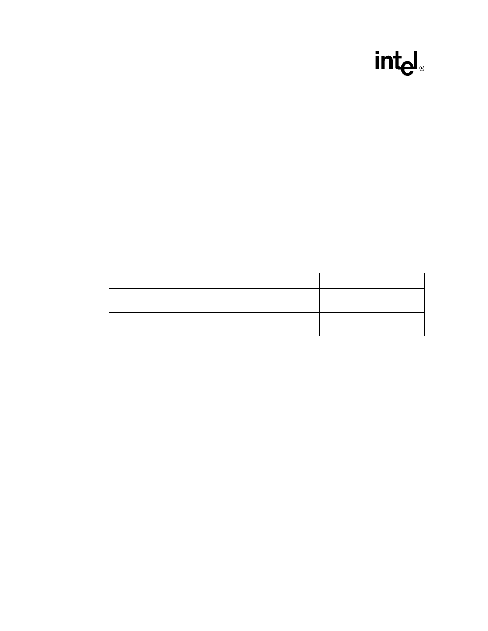
Table 76. Address Map
Start Address
End Address
Responder
0x0000 0000
0x3FFF FFFF
Channel 0
0x4000 0000
0x7FFF FFFF
Channel 1
0x8000 0000
0xBFFF FFFF
Channel 2
0xc000 0000
0xFFFF FFFF
Channel 3