Lock, Tructure – Maxim Integrated DS33Z41 User Manual
Page 24
DS33Z41 Quad IMUX Ethernet Mapper
24 of 167
8.2 Clock
Structure
The DS33Z41 clocks sources and functions are as follows:
• Serial Transmit Data (TCLKI) and Serial Receive Data (RCLKI) clock inputs are used to transfer data from
the serial interface. These clocks can be gapped.
• System Clock (SYSCLKI) input. Used for internal operation. This clock input cannot be a gapped clock. A
clock supply with
±100ppm frequency accuracy is suggested. A buffered version of this clock is provided
on the SDCLKO pin for the operation of the SDRAM. A divided and buffered version of this clock is
provided on REF_CLKO for the RMII/MII interface.
• Packet Interface Reference clock (REF_CLK) input that can be 25MHz or 50MHz. This clock is used as
the timing reference for the RMII/MII interface.
• The Transmit and Receive clocks for the MII Interface (TX_CLK and RX_CLK). In DTE mode, these are
input pins and accept clocks provided by an Ethernet PHY. In the DCE mode, these are output pins and
will output an internally generated clock to the Ethernet PHY. The output clocks are generated by internal
division of REF_CLK. In RMII mode, only the REF_CLK input is used.
• REF_CLKO is an output clock that is generated by dividing the 100MHz System clock (SYSCLKI) by 2 or
4.
• A Management Data Clock (MDC) output is derived from SYSCLKI and is used for information transfer
between the internal Ethernet MAC and external PHY. The MDC clock frequency is 1.67MHz.
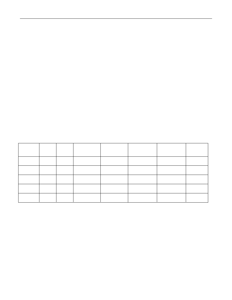
The following table provides the different clocking options for the Ethernet interface.
Table 8-1. Clock Selection for the Ethernet (LAN) Interface
RMIIMIIS
PIN
SPEED
(Mbps)
DCE/
DTE
REF_CLKO
OUTPUT
(MHz)
REF_CLK
INPUT
RX_CLK TX_CLK
MDC
OUTPUT
(MHz)
0 (MII)
10
DTE
25
25MHz
±100ppm
Input from
PHY
Input from
PHY
1.67
0 (MII)
10
DCE
25
25MHz
±100ppm
2.5MHz
(Output)
2.5MHz
(Output)
1.67
0 (MII)
10
DCE
25
25MHz
±100ppm
25MHz
(Output)
25MHz
(Output)
1.67
1 (RMII)
10
—
50
50MHz
±100ppm
Not Applicable Not Applicable
1.67
1 (RMII)
10
—
50
50MHz
±100ppm
Not Applicable Not Applicable
1.67