Maxim Integrated DS33Z41 User Manual
Page 19
DS33Z41 Quad IMUX Ethernet Mapper
19 of 167
NAME PIN
TYPE
FUNCTION
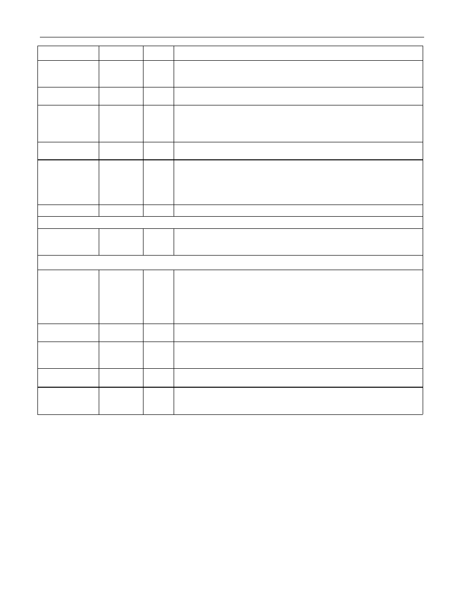
SCAS
H4 O
SDRAM Column Address Strobe. Active-low output, used to latch the
column address on the rising edge of SDCLKO. It is used with
commands for Bank Activate, Precharge, and Mode Register Write.
SWE
M4 O
SDRAM Write Enable. This active-low output enables write operation
and auto precharge.
SDMASK[0]
SDMASK[1]
SDMASK[2]
SDMASK[3]
N6
G4
M10
M9
O
SDRAM Mask 0 to 3. When high, a write is done for that byte. The
least significant byte is SDATA7 to SDATA0. The most significant byte
is SDATA31 to SDATA24.
SDCLKO N5
O
(4mA)
SDRAM CLK Out. System clock output to the SDRAM. This clock is a
buffered version of SYSCLKI.
SYSCLKI G13 I
System Clock In. 100MHz System Clock input to the DS33Z41, used
for internal operation. This clock is buffered and provided at SDCLKO
for the SDRAM interface. The DS33Z41 also provides a divided version
output at the REF_CLKO pin. A clock supply with
±100ppm frequency
accuracy is suggested.
SDCS
L6 O
SDRAM Chip Select. Active-low output enables SDRAM access.
QUEUE STATUS
QOVF C7
O
Queue Overflow. This pin goes high when the transmit or receive
queue has overflowed. This pin will go low when the high watermark is
reached again.
JTAG INTERFACE
JTRST
E6 Ipu
JTAG Reset.
JTRST is used to asynchronously reset the test access
port controller. After power-up, a rising edge on
JTRST will reset the
test port and cause the device I/O to enter the JTAG DEVICE ID mode.
Pulling
JTRST low restores normal device operation. JTRST is pulled
HIGH internally via a 10k
Ω resistor operation. If boundary scan is not
used, this pin should be held low.
JTCLK D4
Ipu
JTAG Clock. This signal is used to shift data into JTDI on the rising
edge and out of JTDO on the falling edge.
JTDO E5
Oz
JTAG Data Out. Test instructions and data are clocked out of this pin
on the falling edge of JTCLK. If not used, this pin should be left
unconnected.
JTDI E4
Ipu
JTAG Data In. Test instructions and data are clocked into this pin on
the rising edge of JTCLK. This pin has a 10k
Ω pullup resistor.
JTMS F7
Ipu
JTAG Mode Select. This pin is sampled on the rising edge of JTCLK
and is used to place the test access port into the various defined IEEE
1149.1 states. This pin has a 10k
Ω pullup resistor.