Jtag functional timing, Jtag f, Unctional – Maxim Integrated DS33Z41 User Manual
Page 165: Iming, 5 jtag functional timing, Figure 12-3. jtag functional timing
DS33Z41 Quad IMUX Ethernet Mapper
165 of 167
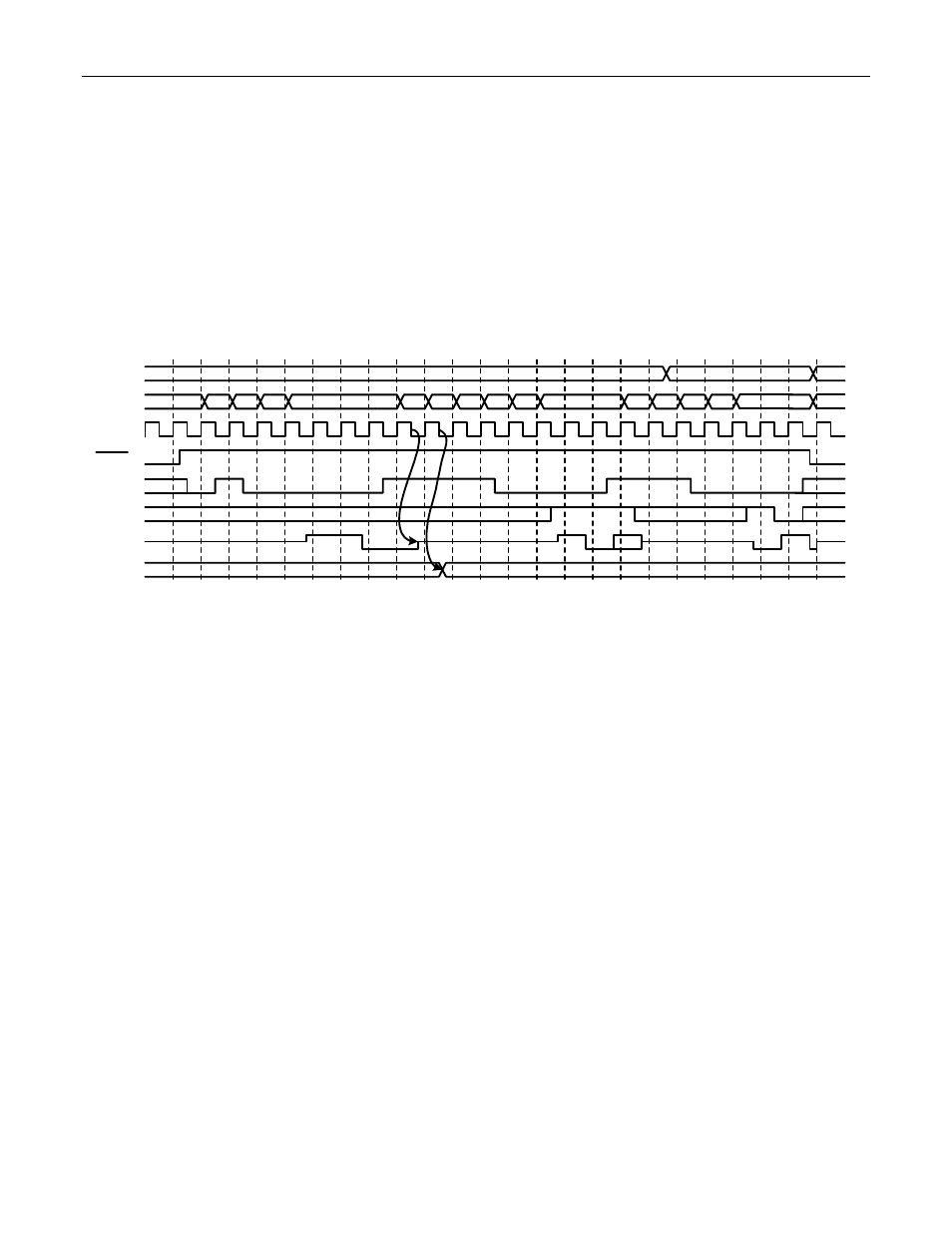
12.5 JTAG Functional Timing
This functional timing for the JTAG circuits shows:
• The JTAG controller starting from reset state.
• Shifting out the first 4 LSB bits of the IDCODE.
• Shifting in the BYPASS instruction (111) while shifting out the mandatory X01 pattern.
• Shifting the TDI pin to the TDO pin through the bypass shift register.
• An asynchronous reset occurs while shifting.
Figure 12-3. JTAG Functional Timing
JTCLK
JTRST
JTMS
JTDI
JTDO
(STATE)
Reset
X
Run Test
Idle
Select DR
Scan
Capture
DR
Shift
DR
Exit1
DR
Update
DR
Select DR
Scan
Select IR
Scan
Capture
IR
Shift IR
Exit1
IR
Update
IR
Select DR
Scan
Capture
DR
Shift
DR
Test
Logic Idle
(INST)
IDCODE
BYPASS
IDCODE
X
X
X
X
X
Output
Pin
Output pin level change if in "EXTEST" instruction mode
- DS80C390 (58 pages)
- DS5001FP (26 pages)
- MAX1416 (14 pages)
- MAX5865 (18 pages)
- MAX1202 (7 pages)
- USBTO232 (31 pages)
- HFAN-09.5.0: Pattern Creator/Converter Software (8 pages)
- MAX-IDE MAXQ Microcontrollers (11 pages)
- MAX6876 Power-Supply Tracker/Sequencer (6 pages)
- MAX6877 Power-Supply Tracker/Sequencer (3 pages)
- 78Q8430 ARM9(920T) Linux Driver Diagnostic Guide (19 pages)
- 78Q8430 Software Driver (54 pages)
- 78Q8430 ST 5100/OS-20 with NexGen TCP/IP Stack (28 pages)
- 6612_OMU_S2_URT_V1_13 (56 pages)
- 6612_OMU_S2+2_URT_V1_14 (58 pages)
- 71M6511 Power Meter IC Family Software (137 pages)
- 71M65xx ADM51 ICE Safety Notice (2 pages)
- 71M6511 2-Layer Demo Board (2 pages)
- 71M6511 4-Layer Demo Board (2 pages)
- 78Q8430 Linux Driver ARM Platform (22 pages)
- 71M6513 Demo Board (2 pages)
- 71M6521DE Energy Meter IC Family Software (138 pages)
- 71M6521 Demo Board (2 pages)
- 71M6531 Demo Board (2 pages)
- 71M6531 Energy Meter IC Family Software (116 pages)
- 71M6533 Demo Board (2 pages)
- 71M6534H Demo Board (2 pages)
- 71M6515H Demo Board (2 pages)
- 73S1209F Evaluation Board (2 pages)
- 73S12xxF (38 pages)
- 73S12xxF Software (93 pages)
- 73S1210F Evaluation Board Lite (2 pages)
- 73S1210F Evaluation Board (2 pages)
- 73S1210F Multi-SAM Evaluation Board Lite (2 pages)
- 73S12xxF USB-CCID Linux DFU Host Application (8 pages)
- 73S1215F Device Firmware Upgrade Host Driver/Application (10 pages)
- 73S12xxF USB-CCID Host GUI (22 pages)
- 73S1215F Windows XP 32 USB CCID and DFU Drivers (15 pages)
- 73S1215F CCID USB Linux Driver (16 pages)
- 73S1215F Evaluation Board (2 pages)
- 73S1215F Evaluation Board Lite (2 pages)
- 73S1217F Evaluation Board (2 pages)
- 73S1217F Evaluation Board Lite (2 pages)
- MAXQ Family (216 pages)