Jtag interface timing, Jtag i, Nterface – Maxim Integrated DS33Z41 User Manual
Page 158: Iming
DS33Z41 Quad IMUX Ethernet Mapper
158 of 167
11.9 JTAG Interface Timing
Table 11-14. JTAG Interface Timing
(VDD3.3 = 3.3V
±5%, VDD1.8 = 1.8V ±5%, Tj = -40°C to +85°C.)
PARAMETER SYMBOL
CONDITIONS
MIN
TYP
MAX
UNITS
JTCLK Clock Period
t1
1000
ns
JTCLK Clock High:Low Time
t2:t3
(Note 1)
50
500
ns
JTCLK to JTDI, JTMS Setup Time
t4
2
ns
JTCLK to JTDI, JTMS Hold Time
t5
2
ns
JTCLK to JTDO Delay
t6
2
50
ns
JTCLK to JTDO HIZ Delay
t7
2
50
ns
JTRST Width Low Time
t8
100 ns
Note 1:
Clock can be stopped high or low.
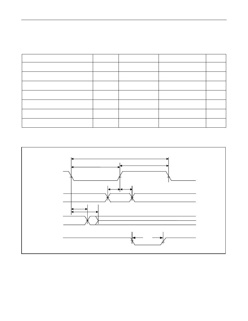
Figure 11-15. JTAG Interface Timing Diagram
JTCLK
t1
JTD0
t4
t5
t2
t3
t7
JTDI, JTMS,
JTRST
t6
JTRST
t8
See also other documents in the category Maxim Integrated Hardware:
- DS80C390 (58 pages)
- DS5001FP (26 pages)
- MAX1416 (14 pages)
- MAX5865 (18 pages)
- MAX1202 (7 pages)
- USBTO232 (31 pages)
- HFAN-09.5.0: Pattern Creator/Converter Software (8 pages)
- MAX-IDE MAXQ Microcontrollers (11 pages)
- MAX6876 Power-Supply Tracker/Sequencer (6 pages)
- MAX6877 Power-Supply Tracker/Sequencer (3 pages)
- 78Q8430 ARM9(920T) Linux Driver Diagnostic Guide (19 pages)
- 78Q8430 Software Driver (54 pages)
- 78Q8430 ST 5100/OS-20 with NexGen TCP/IP Stack (28 pages)
- 6612_OMU_S2_URT_V1_13 (56 pages)
- 6612_OMU_S2+2_URT_V1_14 (58 pages)
- 71M6511 Power Meter IC Family Software (137 pages)
- 71M65xx ADM51 ICE Safety Notice (2 pages)
- 71M6511 2-Layer Demo Board (2 pages)
- 71M6511 4-Layer Demo Board (2 pages)
- 78Q8430 Linux Driver ARM Platform (22 pages)
- 71M6513 Demo Board (2 pages)
- 71M6521DE Energy Meter IC Family Software (138 pages)
- 71M6521 Demo Board (2 pages)
- 71M6531 Demo Board (2 pages)
- 71M6531 Energy Meter IC Family Software (116 pages)
- 71M6533 Demo Board (2 pages)
- 71M6534H Demo Board (2 pages)
- 71M6515H Demo Board (2 pages)
- 73S1209F Evaluation Board (2 pages)
- 73S12xxF (38 pages)
- 73S12xxF Software (93 pages)
- 73S1210F Evaluation Board Lite (2 pages)
- 73S1210F Evaluation Board (2 pages)
- 73S1210F Multi-SAM Evaluation Board Lite (2 pages)
- 73S12xxF USB-CCID Linux DFU Host Application (8 pages)
- 73S1215F Device Firmware Upgrade Host Driver/Application (10 pages)
- 73S12xxF USB-CCID Host GUI (22 pages)
- 73S1215F Windows XP 32 USB CCID and DFU Drivers (15 pages)
- 73S1215F CCID USB Linux Driver (16 pages)
- 73S1215F Evaluation Board (2 pages)
- 73S1215F Evaluation Board Lite (2 pages)
- 73S1217F Evaluation Board (2 pages)
- 73S1217F Evaluation Board Lite (2 pages)
- MAXQ Family (216 pages)