Operating parameters, 11 operating parameters, Absolute maximum ratings – Maxim Integrated DS33Z41 User Manual
Page 142: Table 11-1. recommended dc operating conditions, Table 11-2. dc electrical characteristics
DS33Z41 Quad IMUX Ethernet Mapper
142 of 167
11 OPERATING PARAMETERS
ABSOLUTE MAXIMUM RATINGS
Voltage Range on Any Lead with Respect to V
SS
(except V
DD
)………………………………………….–0.5V to +5.5V
Supply Voltage (VDD3.3) Range with Respect to V
SS
.……………………………………………………–0.3V to +3.6V
Supply Voltage (VDD1.8) Range with Respect to V
SS
….…………………………………………………–0.3V to +2.0V
Ambient Operating Temperature Range………………………………………………...…………………–40ºC to +85ºC
Junction Operating Temperature Range…………………………………………………..……………..–40ºC to +125ºC
Storage Temperature………………………………………………………………………….……………–55ºC to +125ºC
Soldering Temperature………………………………………………………..See IPC/JEDEC J-STD-020 specification
These are stress ratings only and functional operation of the device at these or any other conditions beyond those indicated in the operation
sections of this specification is not implied. Exposure to absolute maximum rating conditions for extended periods of time can affect reliability.
Ambient Operating Temperature Range is assuming the device is mounted on a JEDEC standard test board in a convection cooled JEDEC
test enclosure.
Note: The “typ” values listed below are not production tested.
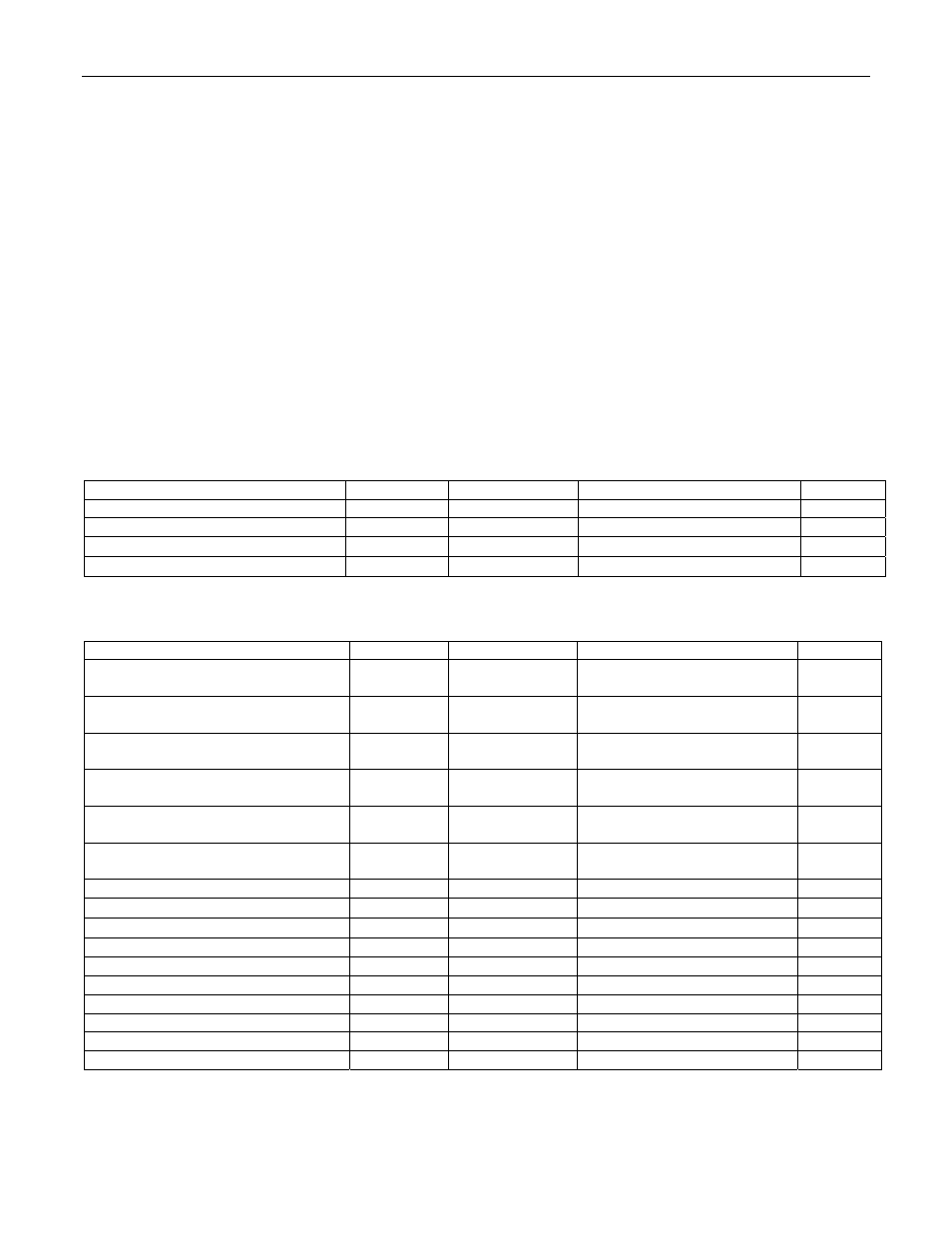
Table 11-1. Recommended DC Operating Conditions
(VDD3.3 = 3.3V
±5%, VDD1.8 = 1.8 ±5% T
j
= -40°C to +85°C.)
PARAMETER SYMBOL
CONDITIONS
MIN
TYP
MAX
UNITS
Logic 1
V
IH
2.0
3.465
V
Logic 0
V
IL
-0.3
+0.8
V
Supply (VDD3.3)
±5%
VDD3.3
3.135 3.300 3.465
V
Supply(VDD1.8)
±5%
VDD1.8
1.71 1.8 1.89 V
Table 11-2. DC Electrical Characteristics
(VDD3.3 = 3.3V
±5%, VDD1.8 = 1.8 ±5% T
j
= -40°C to +85°C.)
PARAMETER
SYMBOL CONDITIONS MIN TYP MAX UNITS
I/O Supply Current
(VDD3.3 = 3.465V)
I
ddio
(Notes 1, 2)
35
125
mA
Core Supply Current
(VDD1.8 = 1.89)
I
ddcore
(Notes 1, 2)
35
125
mA
I/O Standby Current in Reset
(VDD3.3 = 3.465V)
I
DDD
(Notes 2, 3)
15
mA
Core Standby Current in Reset
(VDD1.8 = 1.89)
I
DDDCORE
(Notes 2, 3)
35
mA
I/O Static Current
(VDD3.3 = 3.465V)
I
DDD
(Notes 2, 4)
15
30
mA
Core Static Current
(VDD1.8 = 1.89)
I
DDDCORE
(Notes 2, 4)
0.2
2
mA
Lead Capacitance
C
IO
7
pF
Input Leakage
I
IL
-10 +10
µA
Input Leakage
I
ILP
-50 -10
µA
Output Leakage (when Hi-Z)
I
LO
-10
+10
µA
Output Voltage (I
OH
= -4.0mA)
V
OH
All
Outputs
2.4
V
Output Voltage (I
OL
= +4.0mA)
V
OL
All
Outputs
0.4 V
Output Voltage (I
OH
= -8.0mA)
V
OH
REF_CLKO
2.4
V
Output Voltage (I
OL
= +12.0mA)
V
OL
TSER
0.4 V
Input Voltage
V
IL
0.8 V
Input Voltage
V
IH
2.0
V