NEC PD75402A User Manual
Page 86

75
CHAPTER 5. PERIPHERAL HARDWARE FUNCTIONS
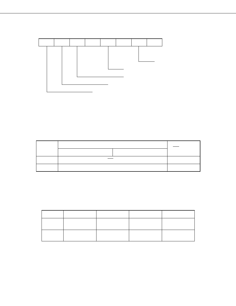
Fig. 5-25 Serial Operating Mode Register (CSIM) Format (1/2)
Address
7
6
5
4
3
2
1
0
Symbol
FE0H
CSIE
COI
WUP
0
CSIM3
0
CSIM1
0
CSIM
Serial Clock Selection Bit (W)
Serial Interface Operating Mode Selection Bit (W)
Wake-up Function Specification Bit (W)
Signal from Address Comparator (R)
Serial Interface Operation Enable/Disable Specification Bit (W)
Remarks
(R) Read only
(W) Write only
Note
0 must be written to CSIM bits 4, 2, 0.
Serial clock selection bit (W)
Serial Clock
CSIM1
SCK Pin Mode
3-Wire Serial I/O Mode
SBI Mode
0
Input clock to SCK pin from off chip
Input
1
f
XX
/2
4
(262 kHz)
Output
Remarks
( ) When f
XX
= 4.19 MHz
Serial interface operating mode selection bit (W)
Shift Register
Bit Order
CSIM3
Operating Mode
SO Pin Function
SI Pin Function
0
1
3-wire serial
I/O mode
SBI mode
SIO
7 to 0
↔
XA
(MBS-first transfer)
SIO
7 to 0
↔
XA
(MBS-first transfer)
SO/P02
(CMOS output)
SB0/P02
(N-ch open-drain
input/output)
SI/P03
(Input)
P03 input
