NEC PD75402A User Manual
Page 142

131
CHAPTER 6. INTERRUPT FUNCTIONS
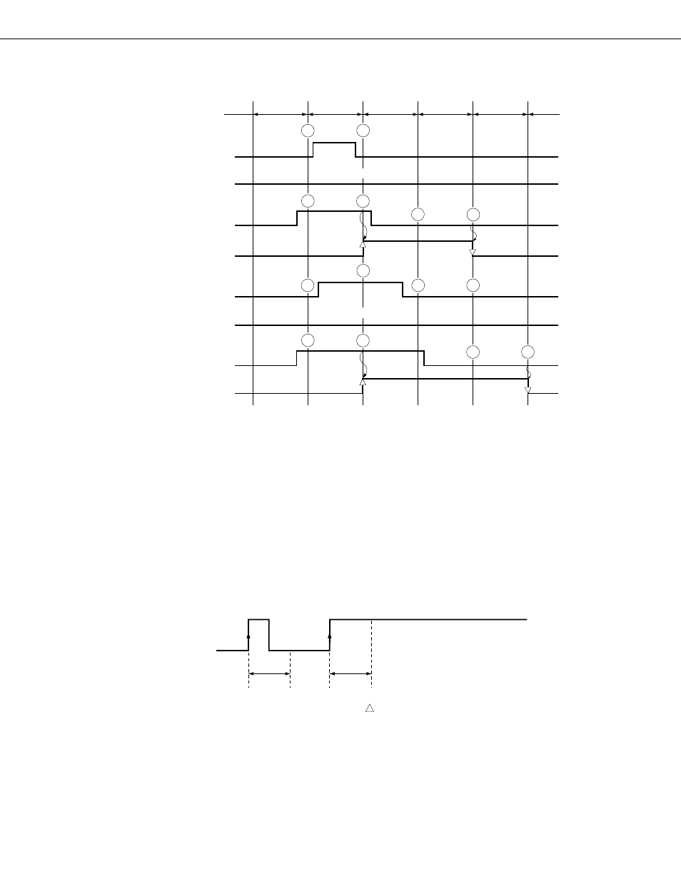
Fig. 6-4 INT0 Noise Elimination Circuit Input/Output Timing
Remarks
t
SMP
= t
CY
or 64/f
XX
Specification of the detected edge of the INT0 input and selection of the sampling clock is performed by the edge
detection mode register (IM0).
As signals are also input via the noise elimination circuit when the INT0 pin inputs data as a port, the input data
must be of sufficient width to avoid being eliminated as noise.
INT2 functions as an externally testable input which sets a testable flag on detection of a rising edge. Noise
elimination by the sampling clock is not performed, but as there is a function for eliminating pulses which are
narrower than the analog delay, a signal of adequate width must be input as in the case of INT0 (see Fig. 6-5).
Fig. 6-5 INT2 Input Noise Elimination
Analog
Delay
Analog
Delay
INT2 Input
Eliminated
as Noise
INT2 Input
Received
Eliminated as Noise
H
H
L
L
L
L
H
H
L
L
L
H
L
L
Eliminated as Noise
t
SMP
t
SMP
t
SMP
t
SMP
t
SMP
➀
➁
➂
Sampling Cycle
(t
SMP
) or Less
INT0
Sheped
Output
1 to 2 Times t
SMP
INT0
Sheped
Output
(a)
2 or More Times
t
SMP
INT0
Sheped
Output
INT0
Sheped
Output
(b)
