NEC PD75402A User Manual
Page 41
CHAPTER 3. FEATURES OF ARCHITECTURE AND MEMORY MAP
30
* 1
* 2
* 3
W
W
W
R
R
R
R
R/W
R/W
R/W
R/W
R/W
R/W
R/W
R/W
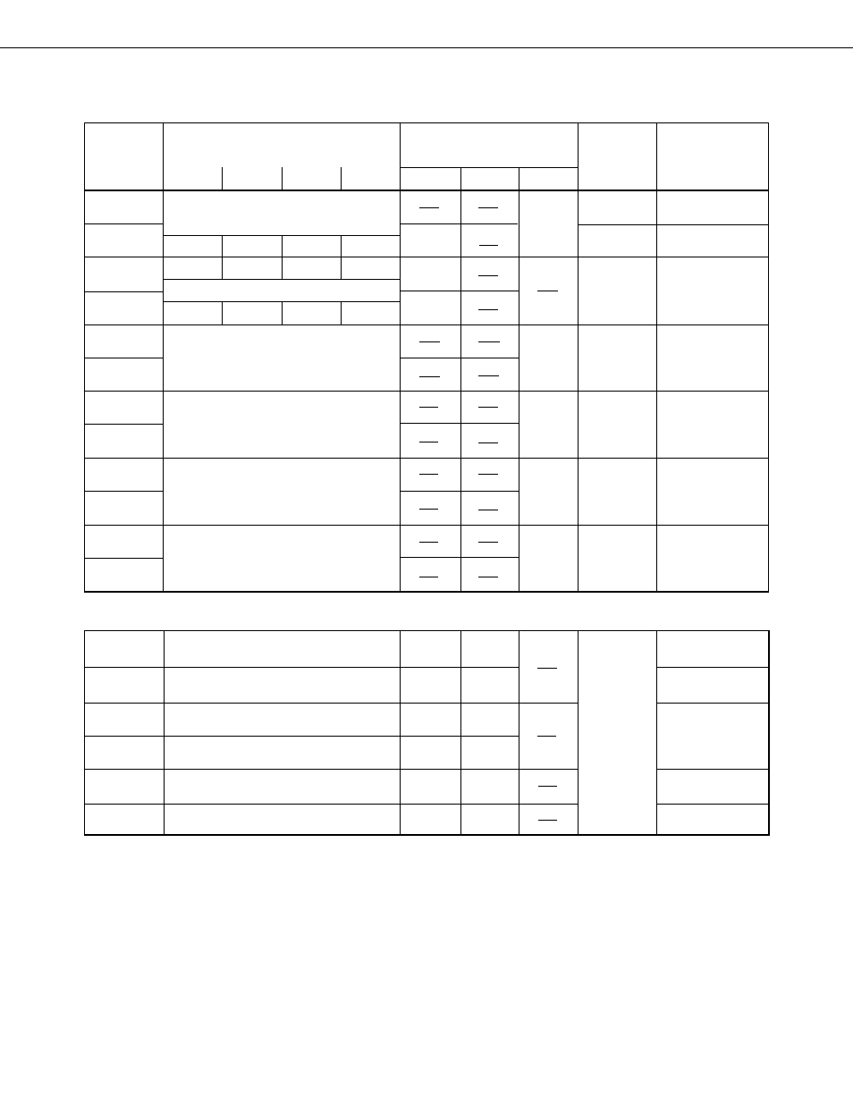
Port 0 (PORT 0)
Port 1 (PORT 1)
Port 2 (PORT 2)
Port 3 (PORT 3)
Port 5 (PORT 5)
Port 6 (PORT 6)
FF0H
FF1H
FF2H
FF3H
FF5H
FF6H
R/W
Serial operation mode register (CSIM)
Table 3-4
µ
PD75402A I/O Map (2/2)
FE0H
FE1H
FE2H
FE3H
FE4H
FE6H
FE8H
FECH
b3
b2
b1
b0
Address
1 Bit
4 Bits
8 Bits
Remarks
Bit
Manipula-
tion
No. of Manipulatable
Addressing
Hardware Name (Symbol)
CSIE
COI
WUP
0
CMDD
RELD
CMDT
RELT
SBI control register (SBIC)
BSYE
ACKD
ACKE
ACKT
W
mem. bit
0 must always be
written in bit 0.
mem. bit
Bit manipulation
only is possible
for all the bits.
11000 must
always be written
in the high-order
5 bits.
Serial I/O shift register (SIO)
Slave address register (SVA)
Port mode register Group A (PMGA)
Port mode register Group B (PMGB)
fmem. bit
*
1. Bits 3 and 1: W; bit 2: R.
2. Bits 3 and 2: R; bits 1 and 0: W.
3. Bits 3 and 1: R/W; bit 2: R; bit 0: W.
Bits 3 and 1 are
fixed to 0.