Clock generation circuit, Clock generation circuit configuration – NEC PD75402A User Manual
Page 65

54
CHAPTER 5. PERIPHERAL HARDWARE FUNCTIONS
5.2
CLOCK GENERATION CIRCUIT
The clock generation circuit supplies various clocks to the CPU and peripheral hardware, and controls the
operating mode of the CPU.
5.2.1
Clock Generation Circuit Configuration
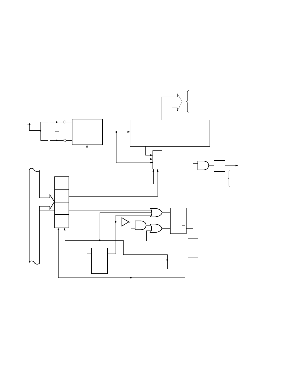
The configuration of the clock generation circuit is shown in Fig. 5-10.
Fig. 5-10 Clock Generation Circuit Block Diagram
Remarks
1.
f
XX
= System clock frequency
2.
f
X
= External clock frequency
3.
PCC: Processor clock control register
4.
1 clock cyck (f
CY
) of
Φ
is 1 machine cycle of an instruction.
*
Instruction execution
★
Internal Bus
V
DD
X1
X2
System
Clock
Oscillation
Circuit
f
XX
or f
X
STOP
Oscillation
1/2 1/16
1/16 to 1/512
Frequency Divider
Selector
Frequency
Divider
• CPU
• INT0 Noise
Eliminator
• Clock Output
Circuit
Φ
HALT F/F
S
R
Q
RESET Input Falling Edga
Detection Signal
RESET Input Rising Edge
Detection Signal
Standby Release Signal from
Interrupt Control Circuit
STOP F/F
Q
S
R
Clear
all bits
Clear
PCC2
PCC0
PCC1
PCC2
PCC3
HALT*
STOP*
PCC
• Basic Interva Timer (BT)
• Clock Output Circuit
• Serial Interface
• INT0 Noise Eliminator
• Clock Output Circuit
4
1/4
