NEC PD75402A User Manual
Page 122
111
CHAPTER 5. PERIPHERAL HARDWARE FUNCTIONS
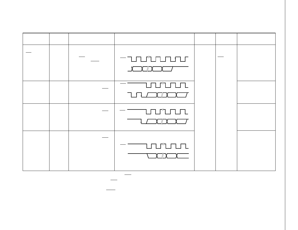
Table 5-8 Signals in SBI Mode (2/2)
Signal Name
Output
Device
Timing Chart
Definition
Output
Condition
Effect on
Flag
Meaning of
Signal
Timing of signal output
to serial data bus
Address value of slave
device on serial bus
Directive, meddage,
etc., to slave device.
Data to ve processed by
slave or master device
Master
Master
Master
Master/
slave
IRQCSI set
(rise of 9th
SCK clock
cycle) *1
Exection of
instruction
to write to
SIO when
CSIE = 1
(serial
transfer
start
directive) *2
Serial Clock
(SCK)
Address
(A7 to A0)
Command
(C7 to C0)
Data
(D7 to D0)
1
2
7
8
9
10
SB0
SCK
SB0
REL
CMD
1
2
7
8
SCK
SCK
SB0
CMD
1
2
7
8
SCK
1
SB0
2
7
8
Synchronization clock for
output of address/command/
data, ACK signal,
Synchronous BUSY signal,
etc.
Address/command/ data is
transferred in first 8 cycles.
8-bit data transferred in
synchronization with SCK
after REL signl and CMD
signal output.
8-bit data transferred in
synchronization with SCK
after CMD signal only is
output without output of REL
signal.
8-bit data transferred in
synchronization with SCK
with no output of either REL
signal or CMD signal.
*
1. When WUP = 0, IRQCSI is always set on the 9th rise of SCK.
When WUP = 1, IRQCSI is set on the 9th rise of SCK only with an address is receive and that address matches the value of the slave address register
(SVA).
2. In data transmission/reception, when in the BUSY stare, the transfer starts after transition to the READY state.