Digital input/output port handling instructions – NEC PD75402A User Manual
Page 58

47
CHAPTER 5. PERIPHERAL HARDWARE FUNCTIONS
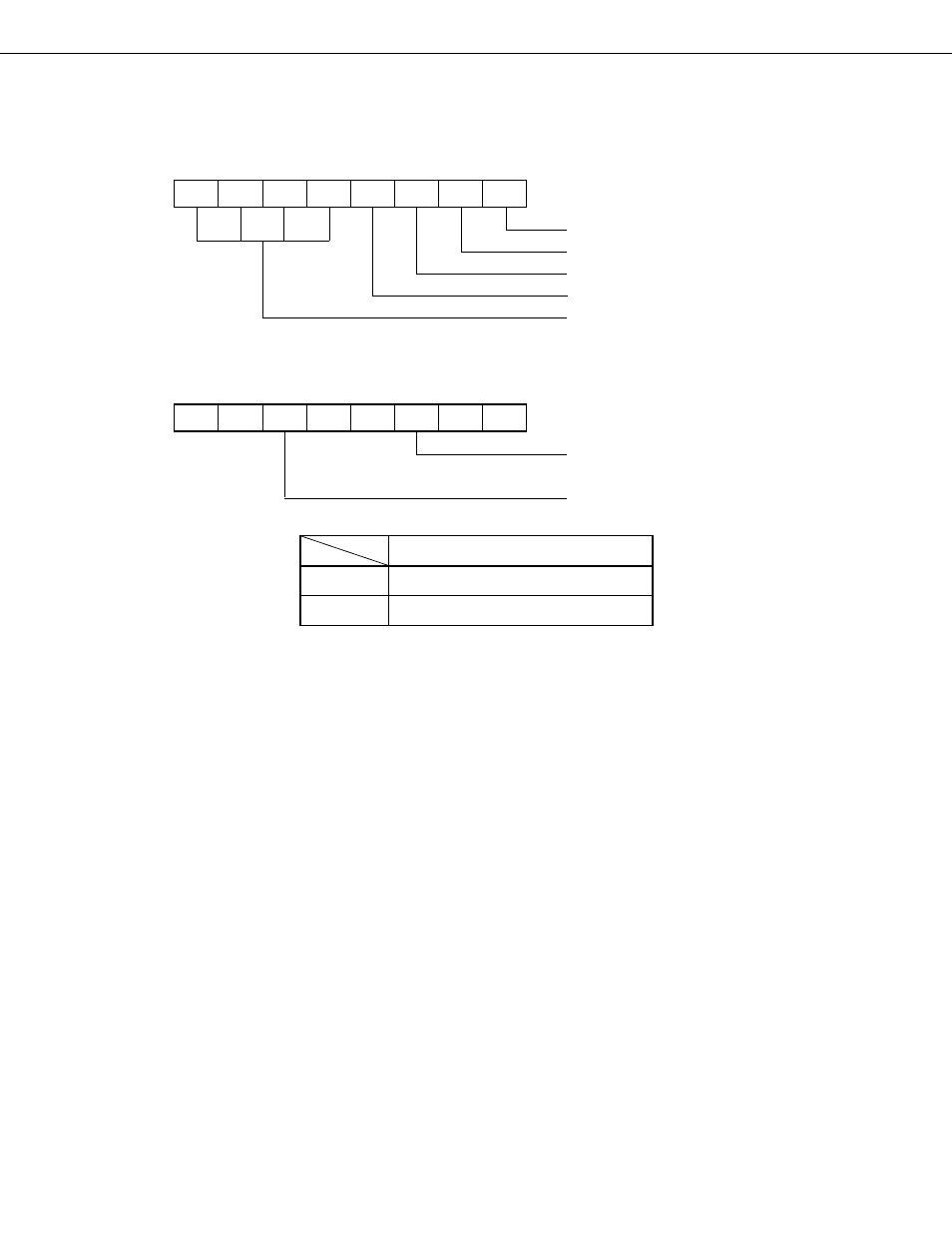
Fig. 5-6 Format of Port Mode Registers
Port Mode Register Group A
Port Mode Register Group B
Specification
0
Input mode (output buffer off)
1
Output mode (output buffer on)
Address
7
6
5
4
3
2
1
0
Symbol
FE8H
PM63 PM62 PM61 PM60 PM33 PM32 PM31 PM30
PMGA
P30 Input/Output Specification
P31 Input/Output Specification
P32 Input/Output Specification
P33 Input/Output Specification
Port 6 (P60 to P63) Input/Output Specification*
Address
7
6
5
4
3
2
1
0
Symbol
FECH
—
—
PM5
—
—
PM2
—
—
PMGB
Port 2 (P20 to P23) Input/Output Specification
Port 5 (P50 to P53) Input/Output Specification
*
Port 6 input/output specification is performed as a 4-bit unit. Ensure that 0000 or 1111 is written to PMGA bits
7 through 4.
5.1.3
Digital Input/Output Port Handling Instructions
As all the input/output ports in the
µ
PD75402A are mapped onto data memory space, all data memory handling
instructions can be used. Those data memory handling instructions which are considered particularly useful for
input/output pin operations are shown in Table 5-2 together with their scope of application.
